AD7656-1/AD7657-1/AD7658-1
Data Sheet
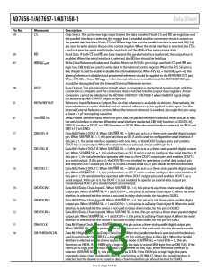
Pin No.
Mnemonic
Description
19
CS
Chip Select. This active low logic input frames the data transfer. If both CS and RD are logic low and
the parallel interface is selected, the output bus is enabled and the conversion result is output on
the parallel data bus lines. If both CS and WR are logic low and the parallel interface is selected, DB[15:8]
are used to write data to the on-chip control register. When the serial interface is selected, the CS is
used to frame the serial read transfer and clock out the MSB of the serial output data.
20
63
RD
Read Data. If both CS and RD are logic low and the parallel interface is selected, the output bus is
enabled. When the serial interface is selected, the RD line should be held low.
Write Data/Reference Enable and Disable. When the H/S SEL pin is high and both CS and WR are
logic low, DB[15:8] are used to write data to the internal control register. When the H/S SEL pin is
WR/REFEN/DIS
DIS
low, this pin is used to enable or disable the internal reference. When H/S SEL = 0 and REFEN/ = 0, the
internal reference is disabled and an external reference should be applied to the REFIN/REFOUT pin.
When H/S SEL = 0 and REFEN/DIS = 1, the internal reference is enabled and the REFIN/REFOUT pin
should be decoupled. See the Internal/External Reference section.
18
51
61
17
BUSY
Busy Output. This pin transitions to high when a conversion is started and remains high until the
conversion is complete and the conversion data is latched into the output data registers. A new
conversion cannot be initiated on the AD7656-1/AD7657-1/AD7658-1 when the BUSY signal is high
because any applied CONVST edges are ignored.
Reference Input/Reference Output. The on-chip reference is available via this pin. Alternatively, the
internal reference can be disabled and an external reference can be applied to this input. See the
Internal/External Reference section. When the internal reference is enabled, decouple this pin using
at least a 1 µF decoupling capacitor.
Serial/Parallel Selection Input. When this pin is low, the parallel interface is selected. When this pin is high,
the serial interface is selected. When the serial interface is selected, DB[10:8] function as DOUT[C:A],
DB[0:2] function as DOUT, and DB7 functions as DCEN. When the serial interface is selected, tie DB15 and
DB[13:11] to DGND.
Data Bit 0/Select DOUT A. When SER/PAR SEL = 0, this pin acts as a three-state parallel digital output
pin. When SER/PAR SEL = 1, this pin functions as SEL A and is used to configure the serial interface. If
this pin is 1, the serial interface operates with one, two, or three DOUT output pins and enables
DOUT A as a serial output. When the serial interface is selected, always set this pin to 1.
REFIN/REFOUT
SER/PAR SEL
DB0/SEL A
16
15
DB1/SEL B
DB2/SEL C
Data Bit 1/Select DOUT B. When SER/PAR SEL = 0, this pin acts as a three-state parallel digital output
pin. When SER/PAR SEL = 1, this pin functions as SEL B and is used to configure the serial interface. If
this pin is 1, the serial interface operates with two or three DOUT output pins and enables DOUT B
as a serial output. If this pin is 0, the DOUT B is not enabled to operate as a serial data output pin
and only one DOUT output pin, DOUT A, is used. Unused serial DOUT pins should be left unconnected.
Data Bit 2/Select DOUT C. When SER/PAR SEL = 0, this pin acts as a three-state parallel digital output
pin. When SER/PAR SEL = 1, this pin functions as SEL C and is used to configure the serial interface. If
this pin is 1, the serial interface operates with three DOUT output pins and enables DOUT C as a
serial output. If this pin is 0, the DOUT C is not enabled to operate as a serial data output pin.
Unused serial DOUT pins should be left unconnected.
14
13
12
DB3/DCIN C
DB4/DCIN B
DB5/DCIN A
Data Bit 3/Daisy-Chain Input C. When SER/PAR SEL = 0, this pin acts as a three-state parallel digital
output pin. When SER/PAR SEL = 1 and DCEN = 1, this pin acts as Daisy-Chain Input C. When the serial
interface is selected but the device is not used in daisy-chain mode, tie this pin to DGND.
Data Bit 4/Daisy-Chain Input B. When SER/PAR SEL = 0, this pin acts as a three-state parallel digital
output pin. When SER/PAR SEL = 1 and DCEN = 1, this pin acts as Daisy-Chain Input B. When the serial
interface is selected but the device is not used in daisy-chain mode, tie this pin to DGND.
Data Bit 5/Daisy-Chain Input A. When SER/PAR SEL is low, this pin acts as a three-state parallel digital
output pin. When SER/PAR SEL = 1 and DCEN = 1, this pin acts as Daisy-Chain Input A. When the serial
interface is selected but the device is not used in daisy-chain mode, tie this pin to DGND.
Data Bit 6/Serial Clock. When SER/PAR SEL = 0, this pin acts as a three-state parallel digital output pin.
When SER/PAR SEL = 1, this pin functions as SCLK input and is the read serial clock for the serial transfer.
11
10
DB6/SCLK
DB7/HBEN/DCEN
Data Bit 7/High Byte Enable/Daisy-Chain Enable. When the parallel interface is selected and the device is
used in word mode (SER/PAR SEL = 0 and W/B = 0), this pin functions as Data Bit 7. When the parallel
interface is selected and the device is used in byte mode (SER/PAR SEL = 0 and W/B = 1), this pin
functions as HBEN. If the HBEN pin is logic high, the data is output MSB byte first on DB[15:8]. If the
HBEN pin is logic low, the data is output LSB byte first on DB[15:8]. When the serial interface is
selected (SER/PAR SEL = 1), this pin functions as DCEN. If the DCEN pin is logic high, the parts
operate in daisy-chain mode with DB[5:3] functioning as DCIN[A:C]. When the serial interface is
selected but the device is not used in daisy-chain mode, this pin should be tied to DGND.
Rev. D | Page 12 of 32

 ROCHESTER [ Rochester Electronics ]