AD7656-1/AD7657-1/AD7658-1
Data Sheet
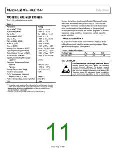
ABSOLUTE MAXIMUM RATINGS
TA = 25°C, unless otherwise noted.
Stresses above those listed under Absolute Maximum Ratings
may cause permanent damage to the device. This is a stress
rating only; functional operation of the device at these or any
other conditions above those indicated in the operational
section of this specification is not implied. Exposure to absolute
maximum rating conditions for extended periods may affect
device reliability.
Table 5.
Parameter
Rating
VDD to AGND, DGND
VSS to AGND, DGND
VDD to AVCC
AVCC to AGND, DGND
DVCC to AVCC
−0.3 V to +16.5 V
+0.3 V to −16.5 V
VCC − 0.3 V to +16.5 V
−0.3 V to +7 V
−0.3 V to AVCC + 0.3 V
−0.3 V to +7 V
THERMAL RESISTANCE
DVCC to DGND, AGND
AGND to DGND
θJA is specified for the worst-case conditions, that is, a device
soldered in a circuit board for surface-mount packages. These
specifications apply to a 4-layer board.
−0.3 V to +0.3 V
VDRIVE to DGND
−0.3 V to DVCC + 0.3 V
VSS − 0.3 V to VDD + 0.3 V
−0.3 V to VDRIVE + 0.3 V
−0.3 V to VDRIVE + 0.3 V
−0.3 V to AVCC + 0.3 V
Analog Input Voltage to AGND1
Digital Input Voltage to DGND
Digital Output Voltage to DGND
REFIN/REFOUT to AGND
Table 6. Thermal Resistance
Package Type
θJA
θJC
Unit
64-Lead LQFP
45
11
°C/W
Input Current to Any Pin Except
Supplies2
Operating Temperature Range
B Version
10 mA
ESD CAUTION
−40°C to +85°C
−40°C to +125°C
−65°C to +150°C
150°C
Y Version
Storage Temperature Range
Junction Temperature
Pb/Sn Temperature, Soldering
Reflow (10 sec to 30 sec)
240(+0)°C
Pb-Free Temperature, Soldering Reflow 260(+0)°C
ESD 1.5 kV
1 If the analog inputs are driven from alternative VDD and VSS supply circuitry,
a 240 Ω series resistor should be placed on the analog inputs and Schottky
diodes should be placed in series with the VDD and VSS supplies of the
AD7656-1/AD7657-1/AD7658-1.
2 Transient currents of up to 100 mA do not cause SCR latch-up.
Rev. D | Page 10 of 32

 ROCHESTER [ Rochester Electronics ]