Data Sheet
AD7656-1/AD7657-1/AD7658-1
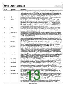
Pin No.
Mnemonic
Description
7
DB8/DOUT A
DB9/DOUT B
DB10/DOUT C
Data Bit 8/Serial Data Output A. When SER/PAR SEL = 0, this pin acts as a three-state parallel digital
output pin. When SER/PAR SEL = 1 and SEL A = 1, this pin functions as DOUT A and outputs serial
conversion data.
6
5
Data Bit 9/Serial Data Output B. When SER/PAR SEL = 0, this pin acts as a three-state parallel digital
output pin. When SER/PAR SEL = 1 and SEL B = 1, this pin functions as DOUT B and outputs serial
conversion data. This configures the serial interface to have two DOUT output lines.
Data Bit 10/Serial Data Output C. When SER/PAR SEL = 0, this pin acts as a three-state parallel digital
output pin. When SER/PAR SEL = 1 and SEL C = 1, this pin functions as DOUT C and outputs serial
conversion data. This configures the serial interface to have three DOUT output lines.
Data Bit 11/Digital Ground. When SER/PAR SEL = 0, this pin acts as a three-state parallel digital
output pin. When SER/PAR SEL = 1, tie this pin to DGND.
4
DB11
2, 3, 64
DB13, DB12, DB15
Data Bit 12, Data Bit 13, Data Bit 15. When SER/PAR SEL = 0, these pins act as three-state parallel
digital input/output pins. When CS and RD are low, these pins are used to output the conversion
result. When CS and WR are low, these pins are used to write to the control register. When SER/PAR
SEL = 1, tie these pins to DGND. For the AD7657-1, DB15 contains a leading 0. For the AD7658-1,
DB15, DB13, and DB12 contain leading 0s.
1
Data Bit 14/Reference Buffer Enable and Disable. When SER/PAR SEL = 0, this pin acts as a three-
state digital input/output pin. For the AD7657-1 and AD7658-1, DB14 contains a leading 0. When
SER/PAR SEL = 1, this pin can be used to enable or disable the internal reference buffers.
DB14/REFBUFEN
/DIS
28
RESET
Reset Input. When set to logic high, this pin resets the AD7656-1/AD7657-1/AD7658-1. In software
mode, the current conversion is aborted and the internal register is set to all 0s. In hardware mode, the
AD7656-1/AD7657-1/AD7658-1 are configured depending on the logic levels on the hardware select
pins. In all modes, the parts should receive a RESET pulse after power-up. The RESET high pulse should
be typically 100 ns wide. The CONVST pin may be held high during the RESET pulse. However, if the
CONVST pin is held low during the RESET pulse, then after the RESET pulse, the AD7656-1/AD7657-1
/AD7658-1 need to receive a complete CONVST pulse to initiate the first conversion; this should consist
of a high-to-low CONVST edge followed by a low-to-high CONVST edge. In hardware mode, the user
can initiate a RESET pulse between conversion cycles, that is, a 100 ns RESET pulse can be applied to
the device after BUSY has transitioned from high to low and the data has been read. The RESET can
then be issued prior to the next complete CONVST pulse. Ensure that in such a case, RESET has
returned to logic low prior to the next complete CONVST pulse.
27
RANGE
Analog Input Range Selection. Logic input. The logic level on this pin determines the input range of
the analog input channels. When this pin is Logic 1 at the falling edge of BUSY, the range for the
next conversion is 2 × VREF. When this pin is Logic 0 at the falling edge of BUSY, the range for the
next conversion is 4 × VREF. In hardware select mode, the RANGE pin is checked on the falling edge
of BUSY. In software mode (H/S SEL = 1), the RANGE pin can be tied to DGND, and the input range is
determined by the RNGA, RNGB, and RNGC bits in the control register.
31
30
24
VDD
VSS
STBY
Positive Power Supply Voltage. This is the positive supply voltage for the analog input section.
Negative Power Supply Voltage. This is the negative supply voltage for the analog input section.
Standby Mode Input. This pin is used to put all six on-chip ADCs into standby mode. The STBY pin is
high for normal operation and low for standby operation.
62
H/S SEL
W/B
Hardware/Software Select Input. Logic input. When H/S SEL = 0, the AD7656-1/AD7657-1/AD7658-1
operate in hardware select mode, and the ADC pairs to be simultaneously sampled are selected
by the CONVST pins. When H/S SEL = 1, the ADC pairs to be sampled simultaneously are selected by
writing to the control register. When the serial interface is selected, CONVST A is used to initiate
conversions on the selected ADC pairs.
Word/Byte Input. When this pin is logic low, data can be transferred to and from the AD7656-1/
AD7657-1/AD7658-1 using the parallel data lines DB[15:0]. When this pin is logic high and the parallel
interface is selected, byte mode is enabled. In this mode, data is transferred using Data Lines DB[15:8],
and DB 7 functions as HBEN. To obtain the 16-bit conversion result, 2-byte reads are required. When
the serial interface is selected, tie this pin to DGND.
29
Rev. D | Page 13 of 32

 ROCHESTER [ Rochester Electronics ]