Rx5C348A/B
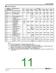
ꢀ Address Mapping
Address
A3A2A1A0
0 0 0 0 0
Register Name
D a t a
D3
S8
D7
-
D6
S40
D5
S20
D4
S10
D2
S4
D1
S2
D0
S1
Second Counter
*2)
1 0 0 0 1
2 0 0 1 0
Minute Counter
Hour Counter
-
-
M40
-
M20
H20
P⋅/A
-
M10
H10
M8
H8
M4
H4
M2
H2
M1
H1
3 0 0 1 1
4 0 1 0 0
Day-of-week Counter
Day-of-month
Counter
-
-
-
-
-
-
D8
W4
D4
W2
D2
W1
D1
D20
D10
5 0 1 0 1
Month Counter and
Century Bit
-
-
MO10 MO8
MO4 MO2
MO1
/19⋅20
6 0 1 1 0
7 0 1 1 1
Year Counter
Oscillation
Y80
(0)
Y40
F6
Y20
F5
Y10
F4
Y8
F3
Y4
F2
Y2
F1
Y1
F0
Adjustment
*4)
Register *3)
8 1 0 0 0
9 1 0 0 1
A 1 0 1 0
Alarm_W
(Minute Register)
Alarm_W
(Hour Register)
-
-
-
WM40 WM20
WM10
WM8 WM4 WM2
WH4 WH2
WW3 WW2 WW1
WM1
WH1
WW0
-
WH20
WP⋅/ A
WW5
WH10 WH8
Alarm_W
WW6
WW4
(Day-of-week
Register)
B 1 0 1 1
C 1 1 0 0
Alarm_D
(Minute Register)
Alarm_D
(Hour Register)
-
-
-
DM40
DM20
DM10
DH10
-
DM8
DH8
-
DM4 DM2
DM1
DH1
-
DH20
DP⋅/A
-
DH4
DH2
D 1 1 0 1
E 1 1 1 0
-
-
-
-
Control Register
*3)
Control Register
*3)
1
2
WALE DALE
/CLEN2 TEST
*5)
XSTP /CLEN1 CTFG WAFG DAFG
*5)
CT2
CT1
CT0
/12⋅24
F 1 1 1 1
VDSL VDET
SCRA
TCH1
Notes:
* 1) All the data listed above accept both reading and writing.
* 2) The data marked with "-" is invalid for writing and reset to 0 for reading.
* 3) When the XSTP bit is set to 1 in Control Register 2, all the bits are reset to 0 in Oscillation Adjustment
Register, Control Register 1 and Control Register 2 excluding the XSTP bit.
* 4) Writing to the Oscillation Adjustment Register requires filling the (0) bit.
* 5) These bit names apply to the Rx5C348A. For the Rx5C348B the bit names are SCRATCH2 and
SCRATCH3.
12345
Rev.2.01
- 11 -

 RICOH [ RICOH ELECTRONICS DEVICES DIVISION ]