RT6263A/B
Application Information
The output stage of a synchronous buck converter is
composed of an inductor and capacitor, which stores
and delivers energy to the load, and forms a
second-order low-pass filter to smooth out the switch
node voltage to maintain a regulated output voltage.
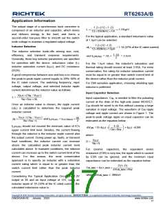
1.2 121.2
12650kHz1A
1.66μH
L
For the typical application, a standard inductance value
of 1.5H can be selected.
1.2 121.2
12650kHz1.5μH
Inductor Selection
I =
L
= 1.1A (37% of the IC rated current)
The inductor selection trade-offs among size, cost,
efficiency, and transient response requirements.
Generally, three key inductor parameters are specified
for operation with the device: inductance value (L),
inductor saturation current (ISAT), and DC resistance
(DCR).
1.1A
2
and I
= 3A +
= 3.55A
L(PEAK)
For the 1.5H value, the inductor's saturation and
thermal rating should exceed at least 3.55A. For more
conservative, the rating for inductor saturation current
must be equal to or greater than switch current limit of
the device rather than the inductor peak current.
A good compromise between size and loss is to choose
the peak-to-peak ripple current equals to 20%~50% of
the IC rated current. The switching frequency, input
voltage, output voltage, and selected inductor ripple
current determines the inductor value as follows :
For EMI sensitive application, choosing shielding type
inductor is preferred.
Input Capacitor Selection
VOUT VIN VOUT
L =
Input capacitance, CIN, is needed to filter the pulsating
current at the drain of the high-side power MOSFET.
CIN should be sized to do this without causing a large
variation in input voltage. The waveform of CIN ripple
voltage and ripple current are shown in Figure 1. The
peak-to-peak voltage ripple on input capacitor can be
estimated as the equation below :
V fSW IL
IN
Once an inductor value is chosen, the ripple current
(IL) is calculated to determine the required peak
inductor current.
VOUT VIN VOUT
and IL(PEAK) = IOUT(MAX)
IL
2
IL=
V fSW L
IN
IL(PEAK) should not exceed the minimum value of IC's
upper current limit level. Besides, the current flowing
through the inductor is the inductor ripple current plus
the output current. During power up, faults, or transient
load conditions, the inductor current can increase
above the calculated peak inductor current level
calculated above. In transient conditions, the inductor
current can increase up to the switch current limit of the
device. For this reason, the most conservative
approach is to specify an inductor with a saturation
current rating which is equal to or greater than the
switch current limit rather than the peak inductor
current.
1D
IN
VCIN = DIOUT
+ IOUT ESR
C fSW
where
V
OUT
D =
V η
IN
For ceramic capacitors, the equivalent series
resistance (ESR) is very low, the ripple which is caused
by ESR can be ignored, and the minimum input
capacitance can be estimated as the equation below :
D 1D
C
IN_MIN
= I
OUT_MAX
V
f
CIN_MAX SW
where VCIN_MAX 200mV
Considering the Typical Application Circuit for 1.2V
output at 3A and an input voltage of 12V, using an
inductor ripple of 1A (33% of the IC rated current), the
calculated inductance value is :
Copyright © 2020 Richtek Technology Corporation. All rights reserved.
is a registered trademark of Richtek Technology Corporation.
DS6263A/B-00 January 2020
www.richtek.com
17

 RICHTEK [ RICHTEK TECHNOLOGY CORPORATION ]