RX62N Group, RX621 Group
4. I/O Registers
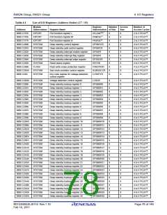
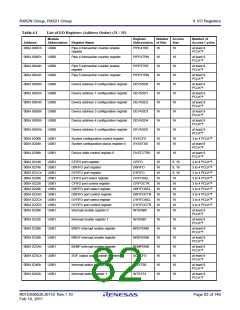
Table 4.1
List of I/O Registers (Address Order) (31 / 35)
Module
Register
Number Access
Number of
Address
Abbreviation Register Name
Abbreviation of Bits
Size
Access Cycles
000A 009Ch
USB0
USB0
USB0
USB0
USB0
USB0
USB0
USB0
USB0
USB0
Pipe 4 transaction counter enable
register
PIPE4TRE
PIPE4TRN
PIPE5TRE
PIPE5TRN
DEVADD0
DEVADD1
DEVADD2
DEVADD3
DEVADD4
DEVADD5
16
16
16
16
16
16
16
16
16
16
16
at least 9
PCLK*9
000A 009Eh
000A 00A0h
000A 00A2h
000A 00D0h
000A 00D2h
000A 00D4h
000A 00D6h
000A 00D8h
000A 00DAh
Pipe 4 transaction counter register
16
16
16
16
16
16
16
16
16
at least 9
PCLK*9
Pipe 5 transaction counter enable
register
at least 9
PCLK*9
Pipe 5 transaction counter register
at least 9
PCLK*9
Device address 0 configuration register
Device address 1 configuration register
Device address 2 configuration register
Device address 3 configuration register
Device address 4 configuration register
Device address 5 configuration register
at least 9
PCLK*9
at least 9
PCLK*9
at least 9
PCLK*9
at least 9
PCLK*9
at least 9
PCLK*9
at least 9
PCLK*9
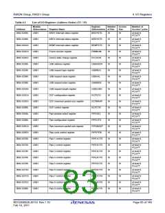
000A 0200h
000A 0204h
USB1
USB1
System configuration control register
System configuration status register 0
SYSCFG
SYSSTS0
16
16
16
16
3 to 4 PCLK*8
at least 9
PCLK*9
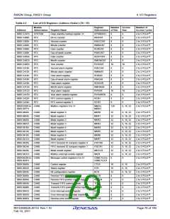
000A 0208h
USB1
Device state control register 0
DVSTCTR0
16
16
at least 9
PCLK*9
000A 0214h
000A 0218h
000A 021Ch
000A 0220h
000A 0222h
000A 0228h
000A 022Ah
000A 022Ch
000A 022Eh
000A 0230h
USB1
USB1
USB1
USB1
USB1
USB1
USB1
USB1
USB1
USB1
CFIFO port register
CFIFO
16
16
16
16
16
16
16
16
16
16
8, 16
8, 16
8, 16
16
3 to 4 PCLK*8
3 to 4 PCLK*8
3 to 4 PCLK*8
3 to 4 PCLK*8
3 to 4 PCLK*8
3 to 4 PCLK*8
3 to 4 PCLK*8
3 to 4 PCLK*8
3 to 4 PCLK*8
D0FIFO port register
D0FIFO
D1FIFO port register
D1FIFO
CFIFO port select register
CFIFO port control register
D0FIFO port select register
D0FIFO port control register
D1FIFO port select register
D1FIFO port control register
Interrupt enable register 0
CFIFOSEL
CFIFOCTR
D0FIFOSEL
D0FIFOCTR
D1FIFOSEL
D1FIFOCTR
INTENB0
16
16
16
16
16
16
at least 9
PCLK*9
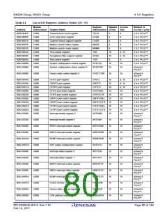
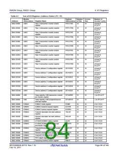
000A 0232h
000A 0236h
000A 0238h
000A 023Ah
000A 023Ch
000A 0240h
000A 0242h
USB1
USB1
USB1
USB1
USB1
USB1
USB1
Interrupt enable register 1
INTENB1
BRDYENB
NRDYENB
BEMPENB
SOFCFG
INTSTS0
INTSTS1
16
16
16
16
16
16
16
16
16
16
16
16
16
16
at least 9
PCLK*9
BRDY interrupt enable register
NRDY interrupt enable register
BEMP interrupt enable register
SOF output configuration register
Interrupt status register 0
at least 9
PCLK*9
at least 9
PCLK*9
at least 9
PCLK*9
at least 9
PCLK*9
at least 9
PCLK*9
Interrupt status register 1
at least 9
PCLK*9
R01DS0052EJ0110 Rev.1.10
Feb 10, 2011
Page 82 of 146

 RENESAS [ RENESAS TECHNOLOGY CORP ]