RX62N Group, RX621 Group
4. I/O Registers
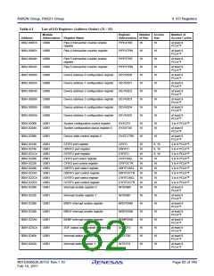
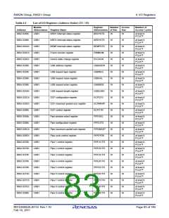
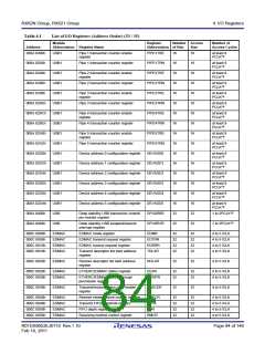
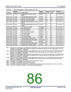
Table 4.1
List of I/O Registers (Address Order) (35 / 35)
Module
Register
Number Access
Number of
Address
Abbreviation Register Name
Abbreviation of Bits
Size
Access Cycles
007F C411h
FLASH
Flash access error interrupt enable
FAEINT
8
8
2 to 3 PCLK*8
register
007F C412h
007F C440h
007F C442h
007F C450h
FLASH
FLASH
FLASH
FLASH
Flash ready interrupt enable register
Data flash read enable register0
Data flash read enable register1
FRDYIE
DFLRE0
DFLRE1
DFLWE0
8
8
2 to 3 PCLK*8
2 to 3 PCLK*8
2 to 3 PCLK*8
2 to 3 PCLK*8
16
16
16
16
16
16
Data flash programming/erasure enable
register0
007F C452h
FLASH
Data flash programming/erasure enable
register1
DFLWE1
16
16
2 to 3 PCLK*8
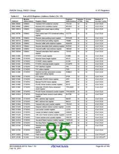
007F C454h
007F FFB0h
007F FFB1h
007F FFB2h
007F FFB4h
007F FFB6h
007F FFBAh
007F FFC8h
007F FFCAh
007F FFCCh
007F FFCEh
007F FFE8h
FLASH
FLASH
FLASH
FLASH
FLASH
FLASH
FLASH
FLASH
FLASH
FLASH
FLASH
FLASH
FCU RAM enable register
Flash status register 0
FCURAME
FSTATR0
FSTATR1
FENTRYR
FPROTR
FRESETR
FCMDR
16
8
16
8
2 to 3 PCLK*8
2 to 3 PCLK*8
2 to 3 PCLK*8
2 to 3 PCLK*8
2 to 3 PCLK*8
2 to 3 PCLK*8
2 to 3 PCLK*8
2 to 3 PCLK*8
2 to 3 PCLK*8
2 to 3 PCLK*8
2 to 3 PCLK*8
2 to 3 PCLK*8
Flash status register 1
8
8
Flash P/E mode entry register
Flash protect register
16
16
16
16
16
16
16
16
16
16
16
16
16
16
16
16
16
16
Flash reset register
FCU command register
FCU processing switching register
Data flash blank check control register
Flash P/E status register
FCPSR
DFLBCCNT
FPESTAT
DFLBCSTAT
PCKAR
Data flash blank check status register
Peripheral clock notification register
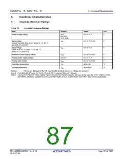
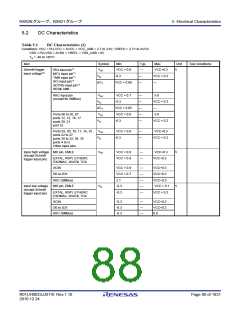
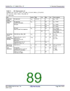
Note 1. When the same output trigger is specified for pulse output groups 2 and 3 by the PPG0.PCR setting, the PPG0.NDRH address
is 000881ECh. When different output triggers are specified, the PPG0.NDRH2 addresses for pulse output groups 2 and 3 are
000881EEh and 000881ECh, respectively.
Note 2. When the same output trigger is specified for pulse output groups 0 and 1 by the PPG0.PCR setting, the PPG0.NDRL address is
000881EDh. When different output triggers are specified, the PPG0.NDRL2 addresses for pulse output groups 0 and 1 are
000881EFh and 000881EDh, respectively.
Note 3. When the same output trigger is specified for pulse output groups 6 and 7 by the PPG1.PCR setting, the PPG1.NDRH address
is 000881FCh. When different output triggers are specified, the PPG1.NDRH2 addresses for pulse output groups 6 and 7 are
000881FEh and 000881FCh, respectively.
Note 4. When the same output trigger is specified for pulse output groups 4 and 5 by the PPG1.PCR setting, the PPG1.NDRL address is
000881FDh. When different output triggers are specified, the PPG1.NDRL2 addresses for pulse output groups 4 and 5 are
000881FFh and 000881FDh, respectively.
Note 5. This register is not supported by the 145-pin TFLGA or 144-pin LQFP version.
Note 6. This register is not supported by the 100-pin LQFP version.
Note 7. This register is not supported by the 85-pin TFLGA version.
Note 8. The number of access states depends on the number of divided cycles for clock synchronization (0 to 1 PCLK, 0 to 1 BCLK).
Note 9. Access may be disabled if a register is accessed during the USB operation.
R01DS0052EJ0110 Rev.1.10
Feb 10, 2011
Page 86 of 146

 RENESAS [ RENESAS TECHNOLOGY CORP ]