RX62N Group, RX621 Group
1. Overview
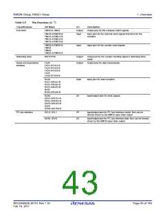
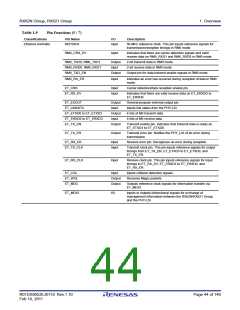
Table 1.9
Pin Functions (5 / 7)
Classifications
Pin Name
I/O
Description
Ethernet controller
REF50CK
Input
50-MHz reference clock. This pin inputs reference signals for
transmission/reception timings in RMII mode.
RMII_CRS_DV
Input
Indicates that there are carrier detection signals and valid
receive data on RMII_RXD1 and RMII_RXD0 in RMII mode.
RMII_TXD0, RMII_TXD1
RMII_RXD0, RMII_RXD1
RMII_TXD_EN
Output
Input
2-bit transmit data in RMII mode.
2-bit receive data in RMII mode.
Output
Output pin for data transmit enable signals in RMII mode.
RMII_RX_ER
Input
Indicates an error has occurred during reception of data in RMII
mode.
ET_CRS
Input
Input
Carrier detection/data reception enable pin.
ET_RX_DV
Indicates that there are valid receive data on ET_ERXD3 to
ET_ERXD0.
ET_EXOUT
Output
Input
General-purpose external output pin.
Inputs link status from the PHY-LSI.
4 bits of MII transmit data.
ET_LINKSTA
ET_ETXD0 to ET_ETXD3
ET_ERXD0 to ET_ERXD3
ET_TX_EN
Output
Input
4 bits of MII receive data.
Output
Transmit enable pin. Indicates that transmit data is ready on
ET_ETXD3 to ET_ETXD0.
ET_TX_ER
Output
Transmit error pin. Notifies the PHY_LSI of an error during
transmission.
ET_RX_ER
ET_TX_CLK
Input
Input
Receive error pin. Recognizes an error during reception.
Transmit clock pin. This pin inputs reference signals for output
timings from ET_TX_EN, ET_ETXD3 to ET_ETXD0, and
ET_TX_ER.
ET_RX_CLK
Input
Receive clock pin. This pin inputs reference signals for input
timings to ET_RX_DV, ET_ERXD3 to ET_ERXD0, and
ET_RX_ER.
ET_COL
ET_WOL
ET_MDC
Input
Inputs collision detection signals.
Receives Magic packets.
Output
Output
Outputs reference clock signals for information transfer via
ET_MDIO.
ET_MDIO
I/O
Inputs or outputs bidirectional signals for exchange of
management information between the RX62N/RX621 Group
and the PHY-LSI.
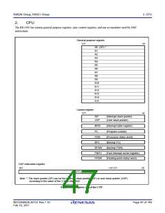
R01DS0052EJ0110 Rev.1.10
Feb 10, 2011
Page 44 of 146

 RENESAS [ RENESAS TECHNOLOGY CORP ]