RX62N Group, RX621 Group
1. Overview
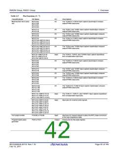
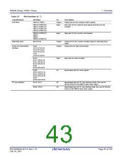
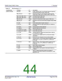
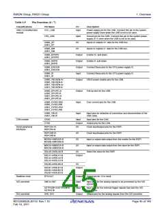
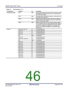
Table 1.9
Pin Functions (4 / 7)
Classifications
Pin Name
I/O
Description
8-bit timer
TMO0 to TMO3
Output
Output pins for the compare match signals.
TMCI0-A/TMCI0-B
TMCI1-A/TMCI1-B
TMCI2-A/TMCI2-B
TMCI3-A/TMCI3-B
Input
Input pins for the external clock signals that drive for the
counters.
TMRI0-A/TMRI0-B
TMRI1
Input
Input pins for the counter-reset signals.
TMRI2
TMRI3-A/TMRI3-B
Watchdog timer
WDTOVF#
Output
Output
Output pin for the counter-overflow signal in watchdog-timer
mode.
Serial communications
interface
TxD0
Output pins for data transmission.
TxD1-A/TxD1-B
TxD2-A/TxD2-B
TxD3-A/TxD3-B
TxD5
TxD6-A/TxD6-B
RxD0
Input
Input pins for data reception.
RxD1-A/RxD1-B
RxD2-A/RxD2-B
RxD3-A/RxD3-B
RxD5
RxD6-A/RxD6-B
SCK0
I/O
Input/output pins for clock signals.
SCK1-A/SCK1-B
SCK2-A/SCK2-B
SCK3-A/SCK3-B
SCK5
SCK6-A/SCK6-B
I2C bus interface
SCL0, SCL1
I/O
I/O
Input/output pins for I2C bus interface clocks. Bus can be
directly driven by the NMOS open drain output.
SDA0, SDA1
Input/output pins for I2C bus interface data. Bus can be directly
driven by the NMOS open drain output.
R01DS0052EJ0110 Rev.1.10
Feb 10, 2011
Page 43 of 146

 RENESAS [ RENESAS TECHNOLOGY CORP ]