RX62N Group, RX621 Group
1. Overview
1.5
Pin Functions
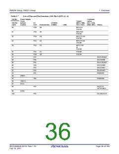
Table 1.8 lists the pin functions.
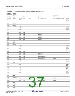
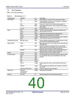
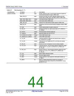
Table 1.9
Pin Functions (1 / 7)
Classifications
Pin Name
I/O
Description
Power supply
VCC
Input
Power supply pin. Connect it to the system power supply.
VCL
Input
Connect this pin to VSS via a 0.1-F capacitor. The capacitor
should be placed close to the pin.
VSS
Input
Input
Ground pin. Connect it to the system power supply (0 V).
PLLVCC
Power supply pin for the PLL circuit. Connect it to the system
power supply.
PLLVSS
XTAL
Input
Ground pin for the PLL circuit.
Clock
Output
Input
Pins for a crystal resonator. An external clock signal can be
input through the EXTAL pin.
EXTAL
BCLK
Output
Output
Output
Input
Outputs the external bus clock for external devices.
Outputs the clock dedicated for the SDRAM.
SDCLK
XCOUT
XCIN
Input/output pins for the subclock generation circuit. Connect a
crystal resonator between XCOUT and XCIN.
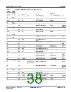
Operating mode control
System control
MD0, MD1, MDE
Input
Pins for setting the operating mode. The signal levels on these
pins must not be changed during operation.
RES#
Input
Input
Reset signal input pin. This LSI enters the reset state when this
signal goes low.
EMLE
Input pin to enable the connection of the on-chip emulator
signal. When the on-chip emulator is used, this pin should be
driven high. When not used, it should be driven low.
BSCANP
Input
Boundary scan pin. Boundary scan is enabled when this pin
goes high. When not used, it should be driven low.
CNVSS
CNVSS
TRST#
TMS
Input
Input
Input
Connect this pin to VSS via pull-down resister.
On-chip emulator
On-chip emulator pins or boundary scan pins. When the EMLE
pin is driven high, these pins are dedicated for the on-chip
emulator.
TDI
Input
TCK
Input
TDO
Output
Output
TRCLK
This pin outputs the clock for synchronization with the trace
data.
TRSYNC
Output
This pin indicates that output from the TRDATA0 to TRDATA3
pins is valid.
TRDATA0-A/TRDATA3-B
Output
Output
These pins output the trace information.
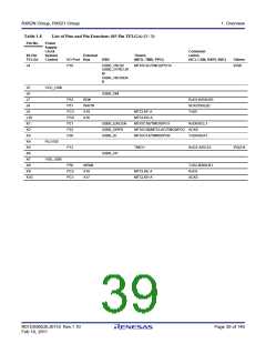
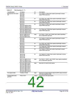
Output pins for the address.
Address bus
Data bus
A0 to A15
A16-A/A16-B to
A23-A/A23-B
D0 to D31
I/O
Input and output pins for the bidirectional data bus.
R01DS0052EJ0110 Rev.1.10
Feb 10, 2011
Page 40 of 146

 RENESAS [ RENESAS TECHNOLOGY CORP ]