RX62N Group, RX621 Group
2. CPU
2.1
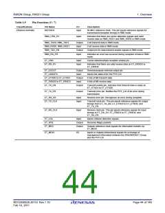
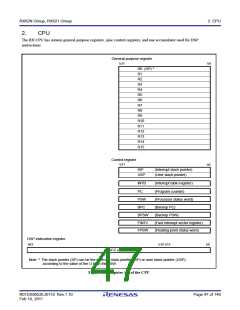
General-Purpose Registers (R0 to R15)
This CPU has sixteen general-purpose registers (R0 to R15). R1 to R15 can be used as data registers or address registers.
R0, a general-purpose register, also functions as the stack pointer (SP). The stack pointer is switched to operate as the
interrupt stack pointer (ISP) or user stack pointer (USP) by the value of the stack pointer select bit (U) in the processor
status word (PSW).
2.2
Control Registers
(1) Interrupt Stack Pointer (ISP)/User Stack Pointer (USP)
The stack pointer (SP) can be either of two types, the interrupt stack pointer (ISP) or the user stack pointer (USP).
Whether the stack pointer operates as the ISP or USP depends on the value of the stack pointer select bit (U) in the
processor status word (PSW).
Set the ISP or USP to a multiple of four, as this reduces the numbers of cycles required to execute interrupt sequences
and instructions entailing stack manipulation.
(2) Interrupt Table Register (INTB)
The interrupt table register (INTB) specifies the address where the relocatable vector table starts.
Set INTB to a multiple of four.
(3) Program Counter (PC)
The program counter (PC) indicates the address of the instruction being executed.
(4) Processor Status Word (PSW)
The processor status word (PSW) indicates results of instruction execution or the state of the CPU.
(5) Backup PC (BPC)
The backup PC (BPC) is provided to speed up response to interrupts.
After a fast interrupt has been generated, the contents of the program counter (PC) are saved in the BPC.
(6) Backup PSW (BPSW)
The backup PSW (BPSW) is provided to speed up response to interrupts.
After a fast interrupt has been generated, the contents of the processor status word (PSW) are saved in the BPSW. The
allocation of bits in the BPSW corresponds to that in the PSW.
(7) Fast Interrupt Vector Register (FINTV)
The fast interrupt vector register (FINTV) is provided to speed up response to interrupts.
The FINTV register specifies a branch destination address when a fast interrupt has been generated.
(8) Floating-Point Status Word (FPSW)
The floating-point status word (FPSW) indicates the results of floating-point operations.
When an exception handling enable bit (Ej) enables the exception handling (Ej = 1), the exception cause can be identified
by checking the corresponding Cj flag in the exception handling routine. If the exception handling is masked (Ej = 0), the
occurrence of exception can be checked by reading the Fj flag at the end of a series of processing. Once the Fj flag has
been set to 1, this value is retained until it is cleared to 0 by software (j = X, U, Z, O, or V).
R01DS0052EJ0110 Rev.1.10
Feb 10, 2011
Page 48 of 146

 RENESAS [ RENESAS TECHNOLOGY CORP ]