RX62N Group, RX621 Group
1. Overview
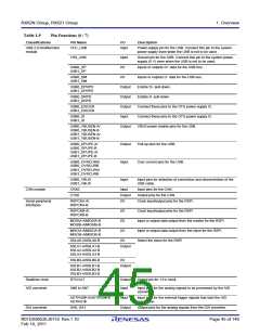
Table 1.9
Pin Functions (6 / 7)
Classifications
Pin Name
I/O
Description
USB 2.0 host/function
module
VCC_USB
Input
Power-supply pin for the USB. Connect this pin to the system
power supply even when the USB is not to be used.
VSS_USB
Input
I/O
Ground pin for the USB. Connect this pin to the system power
supply (0 V) even when the USB is not to be used.
USB0_DP
USB1_DP
Inputs or outputs D+ data for the USB bus.
Inputs or outputs D- data for the USB bus.
Enable D+ pull-down.
USB0_DM
USB1_DM
I/O
USB0_DPRPD
USB1_DPRPD
Output
Output
Output
Input
Output
USB0_DRPD
USB1_DRPD
Enable D- pull-down.
USB0_EXICEN
USB1_EXICEN
Connect these pins to the OTG power supply IC.
Connect these pins to the OTG power supply IC.
VBUS power enable pins for the USB.
USB0_ID
USB1_ID
USB0_VBUSEN-A/
USB0_VBUSEN-B
USB1_VBUSEN-A/
USB1_VBUSEN-B
USB0_DPUPE-A/
USB0_DPUPE-B
USB1_DPUPE-A/
USB1_DPUPE-B
Output
Input
Pull-up pins for the USB.
USB0_OVRCURA/
USB0_OVRCURB
USB1_OVRCURA/
USB1_OVRCURB
Over current pins for the USB.
USB0_VBUS
USB1_VBUS
Input
Input pins for detection of connection and disconnection of the
USB cable.
CAN module
CRX0
CTX0
Input
Output
I/O
Input pins for the CAN.
Output pins for the CAN.
Serial peripheral
interfaces
RSPCKA-A/
RSPCKA-B
Clock input/output pins for the RSPI.
RSPCKB-A/
RSPCKB-B
I/O
I/O
I/O
Clock input/output pins for the RSPI
MOSIA-A/MOSIA-B
MOSIB-A/MOSIB-B
Input or output data output from the master for the RSPI.
Input or output data output from the slave for the RSPI.
Select the slave for the RSPI.
MISOA-A/MISOA-B
MISOB-A/MISOB-B
SSLA0-A/SSLA0-B
I/O
SSLA1-A/SSLA1-B
SSLA2-A/SSLA2-B
SSLA3-A/SSLA3-B
Output
SSLB0-A/SSLB0-B
I/O
SSLB1-A/SSLB1-B
SSLB2-A/SSLB2-B
SSLB3-A/SSLB3-B
Output
Realtime clock
A/D converter
RTCOUT
Output
Input
Output pin for 1-Hz clock.
AN0 to AN7
Input pins for the analog signals to be processed by the A/D
converter.
ADTRG0#-A/ADTRG0#-B
ADTRG1#
Input
Input pins for the external trigger signals that start the A/D
conversion.
D/A converter
DA0, DA1
Output
Output pins for the analog signals from the D/A converter.
R01DS0052EJ0110 Rev.1.10
Feb 10, 2011
Page 45 of 146

 RENESAS [ RENESAS TECHNOLOGY CORP ]