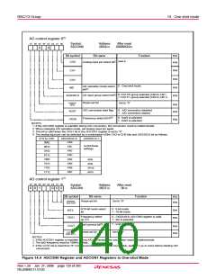
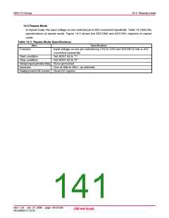
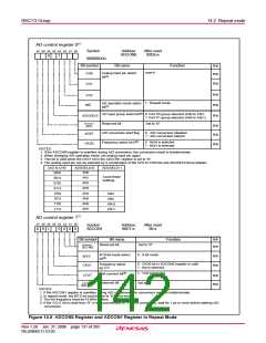
R8C/13 Group
14.5 Internal Equivalent Circuit of Analog Input
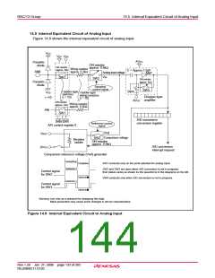
14.5 Internal Equivalent Circuit of Analog Input
Figure 14.8 shows the internal equivalent circuit of analog input.
VCC
VCC VSS
AVCC
Parasitic
diode
ON resistor
ON resistor
approx. 2kΩ
approx. 0.6kΩ
Wiring resistor
C = Approx.1.5pF
AMP
AN0
approx. 0.2k
Ω
Analog input voltage
SW1
VIN
SW2
ON resistor
Parasitic
diode
approx. 5kΩ
Sampling
control signal
SW3
SW4
i ladder-type
V
SS
i ladder-type
wiring resistors
(i = 10)
switches
(i = 10)
Chopper-type
amplifier
i =10
AVSS
ON resistor
Wiring resistor
approx. 2kΩ
approx. 0.2k
Ω
ANi
SW1
A/D successive
conversion register
b2 b1 b0
Reference control
signal
A/D control register 0
Vref
VREF
Comparison voltage
ON resistor
approx. 0.6kΩ
SW2
Resistor
ladder
A/D conversion
interrupt request
AVSS
Comparison reference voltage (Vref) generator
Sampling
SW1 conducts only on the ports selected for analog input.
Comparison
Connect to
SW2 and SW3 are open when A/D conversion is not in progress;
their status varies as shown by the waveforms in the diagrams on the left.
Control signal
for SW2
Connect to
Connect to
SW4 conducts only when A/D conversion is not in progress.
Connect to
Control signal
for SW3
Warning: Use only as a standard for designing this data.
Mass production may cause some changes in device characteristics.
Figure 14.8 Internal Equivalent Circuit to Analog Input
Rev.1.20 Jan 27, 2006 page 133 of 205
REJ09B0111-0120

 RENESAS [ RENESAS TECHNOLOGY CORP ]