R8C/13 Group
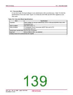
14.2 Repeat mode
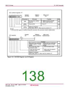
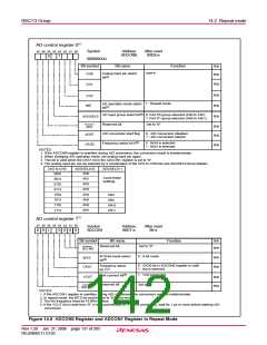
AD control register 0(1)
b7 b6 b5 b4 b3 b2 b1 b0
Symbol
Address
ADCON0
After reset
00D616
1
0
00000XXX
2
Bit symbol
CH0
Bit name
Function
RW
RW
(Note 4)
Analog input pin select
bit(2)
RW
CH1
RW
RW
RW
CH2
MD
1 : Repeat mode
AD operation mode select
bit(2)
AD input group select bit(4)
0: Port P0 group selected (AN
1: Port P1 group selected (AN
0
8
to AN
to AN11
7)
ADGSEL0
)
Reserved bit
Set to “0”
RW
RW
(b5)
A/D conversion start flag
Frequency select bit 0(3)
0 : A/D conversion disabled
1 : A/D conversion started
ADST
0 : fAD/4 is selected
1 : fAD/2 is selected
CKS0
RW
NOTES:
1. If the ADCON0 register is rewritten during A/D conversion, the conversion result is indeterminate.
2. When changing A/D operation mode, set analog input pin again.
3. This bit is valid when the CKS1 bit in the ADCON1 register is set to “0”.
4. The analog input pin can be selected by a combination of the CH2 to CH0 bits and ADGSEL0 bit as follows:
CH2 to CH0
ADGSEL0=0
ADGSEL0=1
AN
AN
AN
AN
AN
AN
AN
AN
0
1
2
3
4
5
6
7
000
001
010
011
100
101
110
111
2
2
2
2
2
2
2
2
Avoid these
settings
AN
AN
8
9
AN10
AN11
(1)
AD control register 1
b7 b6 b5 b4 b3 b2 b1 b0
Symbol
ADCON1
Address
00D716
After reset
0016
0
0
1
0 0 0
0
Bit symbol
(b2-b0)
Bit name
Reserved bit
Function
RW
RW
Set to “0”
8/10-bit mode select
bit(2)
0 : 8-bit mode
RW
RW
BITS
0 : CKS0 bit in ADCON0 register is valid
1 : fAD is selected
Frequency select
bit 1(3)
CKS1
Vref connect bit(4)
1 : Vref connected
VCUT
RW
RW
Reserved bit
Set to “0”
(b6-b7)
NOTES:
1. If the ADCON1 register is rewritten during A/D conversion, the conversion result is indeterminate.
2. In repeat mode, the BITS bit must be set to “0” (8-bit mode).
3. The fAD frequency must be 10 MHz or less.
4. If the VCUT bit is reset from “0” (Vref unconnected) to “1” (Vref connected), wait for 1 µs or more before starting A/D
conversion.
Figure 14.5 ADCON0 Register and ADCON1 Register in Repeat Mode
Rev.1.20 Jan 27, 2006 page 131 of 205
REJ09B0111-0120

 RENESAS [ RENESAS TECHNOLOGY CORP ]