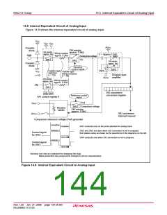
R8C/13 Group
15. Programmable I/O Ports
15. Programmable I/O Ports
15. 1 Description
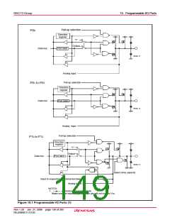
The programmable input/output ports (hereafter referred to as “I/O ports”) consist of 22 lines P0, P1, P30
to P33, P37, and P45. Each port can be set for input or output every line by using a direction register, and
can also be chosen to be or not be pulled high every 4 lines. The port P1 allows the drive capacity of its N-
channel output transistor to be set as necessary. The port P1 can be used as LED drive port if the drive
capacity is set to “HIGH”.
P46 and P47 can be used as an input only port if the main clock oscillation circuit is not used.
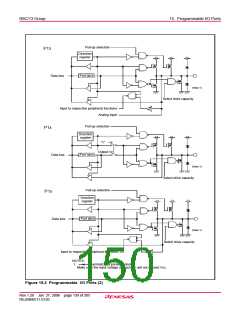
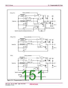
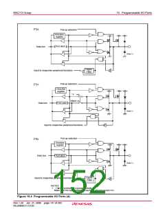
Figures 15.1 to 15.5 show the I/O ports. Figure 15.6 shows the I/O pins.
Each pin functions as an I/O port or a peripheral function input/output.
For details on how to set peripheral functions, refer to each functional description in this manual. If any pin
is used as a peripheral function input, set the direction bit for that pin to “0” (input mode). Any pin used as
an output pin for peripheral functions is directed for output no matter how the corresponding direction bit
is set.
15.1.1 Port Pi Direction Register (PDi Register, i = 0, 1, 3, 4)
Figure 15.7 shows the PDi register.
This register selects whether the I/O port is to be used for input or output. The bits in this register
correspond one for one to each port.
15.1.2 Port Pi Register (Pi Register, i = 0 to 4)
Figure 15.8 shows the Pi register.
Data I/O to and from external devices are accomplished by reading and writing to the Pi register. The
Pi register consists of a port latch to hold the output data and a circuit to read the pin status. For ports
set for input mode, the input level of the pin can be read by reading the corresponding Pi register, and
data can be written to the port latch by writing to the Pi register.
For ports set for output mode, the port latch can be read by reading the corresponding Pi register, and
data can be written to the port latch by writing to the Pi register. The data written to the port latch is
output from the pin. The bits in the Pi register correspond one for one to each port.
15.1.3 Pull-up Control Register 0, Pull-up Control Register 1 (PUR0 and PUR1 Registers)
Figure 15.9 shows the PUR0 and PUR1 registers.
The PUR0 and PUR1 register bits can be used to select whether or not to pull the corresponding port
high in 4 bit units. The port chosen to be pulled high has a pull-up resistor connected to it when the
direction bit is set for input mode.
15.1.4 Port P1 Drive Capacity Control Register (DRR Register)
Figure 15.9 shows the DRR register.
The DRR register is used to control the drive capacity of the port P1 N-channel output transistor. The
bits in this register correspond one for one to each port.
Rev.1.20 Jan 27, 2006 page 137 of 205
REJ09B0111-0120

 RENESAS [ RENESAS TECHNOLOGY CORP ]