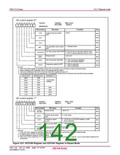
14.7 Output Impedance of Sensor under A/D Conversion
R8C/13 Group
14.7 Output Impedance of Sensor under A/D Conversion
To carry out A/D conversion properly, charging the internal capacitor C shown in Figure 14.11 has to
be completed within a specified period of time. T (sampling time) as the specified time. Let output
impedance of sensor equivalent circuit be R0, microcomputer’s internal resistance be R, precision
(error) of the A/D converter be X, and the A/D converter’s resolution be Y (Y is 1024 in the 10-bit mode,
and 256 in the 8-bit mode).
1
t
–
C (R0 + R)
VC is generally VC = VIN {1 – e
}
X
X
Y
And when t = T, VC=VIN –
VIN = VIN(1 –
)
Y
1
T
X
Y
X
–
C (R0 + R)
e
=
1
–
T = ln
C (R0 +R)
Y
T
Hence, R0 = –
– R
X
C • ln
Y
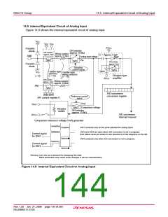
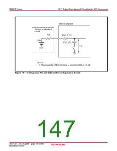
Figure 14.11 shows analog input pin and external sensor equivalent circuit. When the difference
between VIN and VC becomes 0.1 LSB, we find impedance R0 when voltage between pins VC
changes from 0 to VIN – (0.1/1024) VIN in time T. (0.1/1024) means that A/D precision drop due to
insufficient capacitor charge is held to 0.1 LSB at time of A/D conversion in the 10-bit mode. Actual
error however is the value of absolute precision added to 0.1 LSB. When f(XIN) = 10 MHz, T = 0.25 µs
in the A/D conversion mode with sample & hold. Output impedance R0 for sufficiently charging capaci-
tor C within time T is determined as follows.
T = 0.25 µs, R = 2.8 kΩ, C = 1.5 pF, X = 0.1, and Y = 1024 . Hence,
0.25 X 10 –6
R0 = –
– 2.8 X 10³ 7.3 X 10³
0.1
6.0 X 10 –12 • ln
1024
Thus, the allowable output impedance of the sensor circuit capable of thoroughly driving the A/D
converter turns out to be approximately 7.3 kΩ.
Rev.1.20 Jan 27, 2006 page 135 of 205
REJ09B0111-0120

 RENESAS [ RENESAS TECHNOLOGY CORP ]