3858 Group
A/D CONVERTER
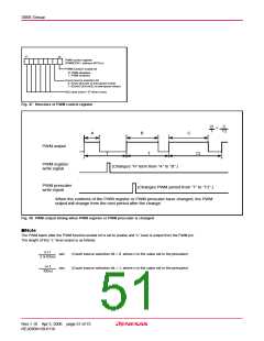
b7
b0
[AD Conversion Register (ADL)] 003516
The A/D conversion register is a read-only register that stores the
result of A/D conversion. Do not read out this register during an A/
D conversion.
AD control register
(ADCON : address 003416, initial value: 1016)
Analog input pin selection bits
0 0 0 0: P30/AN0
0 0 0 1: P31/AN1
0 0 1 0: P32/AN2
0 0 1 1: P33/AN3
0 1 0 0: P34/AN4
0 1 0 1: P04/AN5
0 1 1 0: P05/AN6
0 1 1 1: P06/AN7
1 0 0 0: P07/AN8
[AD Control Register (ADCON)] 003416
The A/D control register controls the A/D converter. Bit 3 to 0 are
analog input pin selection bits. Bit 4 is the AD conversion comple-
tion bit. The value of this bit remains at “0” during A/D conversion,
and changes to “1” at completion of A/D conversion.
AD conversion completion bit
0: Conversion in progress
1: Conversion completed
A/D conversion is started by setting this bit to “0”.
Not used (returns “0” when read)
Comparison Voltage Generator
The comparison voltage generator divides the voltage between
Fig. 49 Structure of AD control register
AVSS and VREF by 256, and outputs the divided voltages.
■Note on A/D converter
Channel Selector
The comparator uses internal capacitors whose charge will be lost
The channel selector selects one of ports P30/AN0 to P34/AN4,
if the clock frequency is too low.
P04/AN5 to P07/AN8 and inputs the voltage to the comparator.
Make sure that f(XIN) is 500 kHz or more during A/D conversion.
As for AD translation accuracy, on the following operating condi-
tions, accuracy may become low.
Comparator and Control Circuit
The comparator and control circuit compare an analog input volt-
age with the comparison voltage, and the result is stored in the AD
conversion registers. When an A/D conversion is completed, the
control circuit sets the AD conversion completion bit and the AD
interrupt request bit to “1”.
(1) Since the analog circuit inside a microcomputer becomes sen-
sitive to noise when VREF voltage is set up lower than Vcc voltage,
accuracy may become low rather than the case where VREF volt-
age and Vcc voltage are set up to the same value..
(2) When VREF voltage is lower than [ 3.0 V ], the accuracy at the
low temperature may become extremely low compared with that at
room temperature. When the system would be used at low tem-
perature, the use at VREF=3.0 V or more is recommended.
Note that because the comparator consists of a capacitor cou-
pling, set f(XIN) to 500 kHz or more during an A/D conversion.
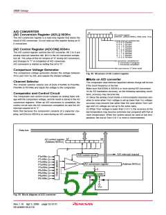
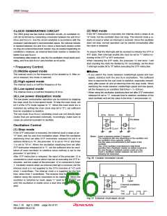
Data bus
b7
4
b0
AD control register
(Address 003416
)
A/D interrupt request
A/D control circuit
P30/AN0
P3
P3
P3
1
2
3
/AN
/AN
/AN
1
2
3
Comparator
AD conversion register
(Address 003516)
P34/AN4
8
P0
P0
4
5
/AN
/AN
5
6
Resistor ladder
P0
P0
6
/AN
7
7
/AN
8
V
REF
VSS
Fig. 50 Block diagram of A/D converter
Rev.1.10 Apr 3, 2006 page 52 of 75
REJ03B0139-0110

 RENESAS [ RENESAS TECHNOLOGY CORP ]