3858 Group
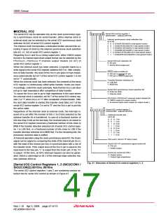
b7
b0
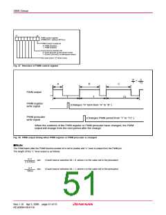
PWM control register
(PWMCON : address 001D16
)
PWM function enable bit
0: PWM disabled
1: PWM enabled
Count source selection bit
0: f(XIN) (f(XCIN) at low-speed mode)
1: f(XIN)/2 (f(XCIN)/2 at low-speed mode)
Not used (return “0” when read)
Fig. 47 Structure of PWM control register
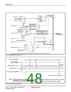
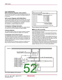
B
T
C
T2
=
A
B
C
PWM output
T
T
T2
PWM register
write signal
(Changes “H” term from “A” to “B”.)
PWM prescaler
write signal
(Changes PWM period from “T” to “T2”.)
When the contents of the PWM register or PWM prescaler have changed, the PWM
output will change from the next period after the change.
Fig. 48 PWM output timing when PWM register or PWM prescaler is changed
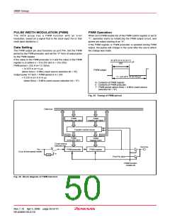
■Note
The PWM starts after the PWM function enable bit is set to enable and “L” level is output from the PWM pin.
The length of this “L” level output is as follows:
n+1
sec
sec
(Count source selection bit = 0, where n is the value set in the prescaler)
(Count source selection bit = 1, where n is the value set in the prescaler)
2 ■ f(XIN)
n+1
f(XIN)
Rev.1.10 Apr 3, 2006 page 51 of 75
REJ03B0139-0110

 RENESAS [ RENESAS TECHNOLOGY CORP ]