3858 Group
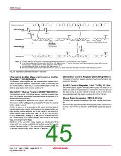
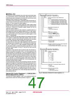
■SERIAL I/O2
b7
b0
Serial I/O2 control register 1
(SIO2CON1 : address 001516
The serial I/O2 can be operated only as the clock synchronous type.
)
As a synchronous clock for serial transfer, either internal clock or
external clock can be selected by the serial I/O2 synchronous clock
selection bit (b6) of serial I/O2 control register 1.
Internal synchronous clock selection bits
b2 b1 b0
0
0
0
0
1
1
0
0
1
1
1
1
0: f(XIN)/8 (f(XCIN)/8 in low-speed mode)
1: f(XIN)/16 (f(XCIN)/16 in low-speed mode)
0: f(XIN)/32 (f(XCIN)/32 in low-speed mode)
1: f(XIN)/64 (f(XCIN)/64 in low-speed mode)
0: f(XIN)/128 f(XCIN)/128 in low-speed mode)
1: f(XIN)/256 (f(XCIN)/256 in low-speed mode)
The internal clock incorporates a dedicated divider and permits se-
lecting 6 types of clock by the internal synchronous clock selection
bits (b2, b1, b0) of serial I/O2 control register 1.
Regarding SOUT2 and SCLK2 being output pins, either CMOS output
format or N-channel open-drain output format can be selected by the
P01/SOUT2, P02/SCLK2 P-channel output disable bit (b7) of
serial I/O2 control register 1.
Serial I/O2 port selection bit
0: I/O port
1: SOUT2,SCLK2 output pin
When the internal clock has been selected, a transfer starts by a
write signal to the serial I/O2 register (address 001716). After comple-
tion of data transfer, the level of the SOUT2 pin goes to high imped-
ance automatically but bit 7 of the serial I/O2 control register 2 is not
set to “1” automatically.
S
0: P0
1: P0
RDY2 output enable bit
3
pin is normal I/O pin
3
pin is SRDY2 output pin
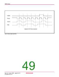
Transfer direction selection bit
0: LSB first
1: MSB first
When the external clock has been selected, the contents of the serial
I/O2 register is continuously sifted while transfer clocks are input.
Accordingly, control the clock externally. Note that the SOUT2 pin does
not go to high impedance after completion of data transfer.
To cause the SOUT2 pin to go to high impedance in the case where
the external clock is selected, set bit 7 of the serial I/O2 control reg-
ister 2 to “1” when SCLK2 is “H” after completion of data transfer. After
the next data transfer is started (the transfer clock falls), bit 7 of the
serial I/O2 control register 2 is set to “0” and the SOUT2 pin is put into
the active state.
Serial I/O2 synchronous clock selection bit
0: External clock
1: Internal clock
P01/SOUT2 ,P02/SCLK2 P-channel output disable bit
0: CMOS output (in output mode)
1: N-channel open-drain output (in output mode )
b7
b0
Serial I/O2 control register 2
(SIO2CON2 : address 001616
)
Regardless of the internal clock to external clock, the interrupt re-
quest bit is set after the number of bits (1 to 8 bits) selected by the
optional transfer bit is transferred. In case of a fractional number of
bits less than 8 bits as the last data, the received data to be stored in
the serial I/O2 register becomes a fractional number of bits close to
MSB if the transfer direction selection bit of serial I/O2 control regis-
ter 1 is LSB first, or a fractional number of bits close to LSB if the
transfer direction selection bit is MSB first. For the remaining bits, the
previously received data is shifted.
Optional transfer bits
b2 b1 b0
0
0
0
0
1
1
1
1
0
0
1
1
0
0
1
1
0: 1 bit
1: 2 bit
0: 3 bit
1: 4 bit
0: 5 bit
1: 6 bit
0: 7 bit
1: 8 bit
At transmit operation using the clock synchronous serial I/O, the SCMP2
signal can be output by comparing the state of the transmit pin SOUT2
with the state of the receive pin SIN2 in synchronization with a rise of
the transfer clock. If the output level of the SOUT2 pin is equal to the
input level to the SIN2 pin, “L” is output from the SCMP2 pin. If not, “H”
is output. At this time, an INT2 interrupt request can also be gener-
ated. Select a valid edge by bit 2 of the interrupt edge selection reg-
ister (address 003A16).
Not used ( returns "0" when read)
Serial I/O2 I/O comparison signal control bit
0: P4
3 I/O
1: SCMP2 output
S
OUT2 pin control bit (P0
0: Output active
1: Output high-impedance
1)
Fig. 41 Structure of Serial I/O2 control registers 1, 2
[Serial I/O2 Control Registers 1, 2 (SIO2CON1 /
SIO2CON2)] 001516, 001616
The serial I/O2 control registers 1 and 2 are containing various se-
lection bits for serial I/O2 control as shown in Figure 41.
Rev.1.10 Apr 3, 2006 page 47 of 75
REJ03B0139-0110

 RENESAS [ RENESAS TECHNOLOGY CORP ]