M37161M8/MA/MF-XXXSP/FP,M37161EFSP/FP
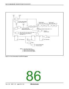
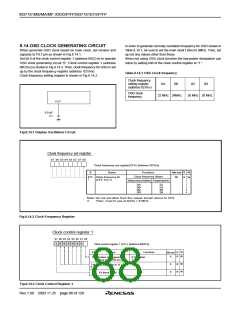
8.14 OSD CLOCK GENERATING CIRCUIT
When generate OSD clock based on main clock, set resistor and
capacity to FILT pin as shown in Fig.8.14.1.
In order to generate normally oscillation frequency for OSD shown in
Table 8.14.1, be sure to set the main clock f (XIN) to 8MHz. Then, set
up not any values other than these.
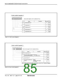
Set bit 0 of the clock control register 1 (address 00CD16) to operate
OSD clock generating circuit “0.” Clock control register 1 (address
00CD16) is shown in Fig.8.14.3. Then, clock frequency for OSD is set
up by the clock frequency register (address 021016).
When not using OSD clock function,the low-power dissipation can
relize by setting bit0 of the clock control register to “1.”
Table.8.14.1 OSD Clock frequency
Clock frequency setting register is shown in Fig.8.14.2.
Clock frequency
0A
0B
setting register
(address 021016
0C
0D
)
OSD clock
frequency
22 MHz 24MHz
26 MHz 28 MHz
FLIT
0.01µF
C1
Fig.8.14.1 Display Oscillation Circuit
Clock frequency set register
b7 b6 b5 b4 b3 b2 b1 b0
Clock frequency set register(CFS) [Address 021016
]
B
Name
Functions
After reset
R
R
W
W
Clock frequency (Note)
0 to
7
Clock frequency bit
(CFS 0 to 7)
0E
Setting value(Limitation) Frequency(MHz)
0A
0B
0C
0D
22
24
26
28
Note: Do not set other than the values shown above to CFS.
Then, must to use at f(X IN) = 8 MHz.
B
Fig.8.14.2 Clock Frequency Register
Clock control register 1
b7 b6 b5 b4 b3 b2 b1 b0
1
0
0
0
0
0
0
Clock control register 1 (CC1) [Address 00CD16
]
B
0
Name
Functions
0:Operation
After reset
W
W
R
R
0
System clock generating
circuit control bit (CC10)
1: Stop
W
W
0
0
R
R
1 to
6
Fix these bits to "0"
Fix these bits to "1"
7
Fig.8.14.3 Clock Control Register 1
Rev.1.00 2003.11.25 page 88 of 128

 RENESAS [ RENESAS TECHNOLOGY CORP ]