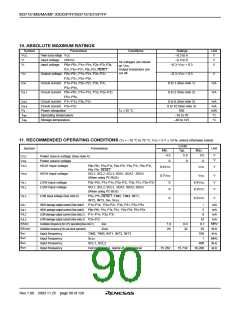
M37161M8/MA/MF-XXXSP/FP,M37161EFSP/FP
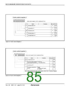
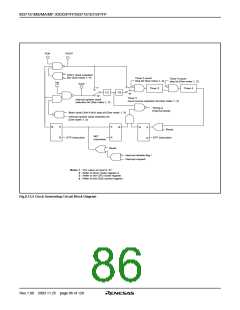
XCIN
XCOUT
OSC1 clock selection
bits (See notes 1, 4)
Timer 3 count
stop bit (See notes 1, 2)
Timer 4 count
stop bit (See notes 1, 2)
XIN
XOUT
“1”
“1”
“0”
Timer 3
Timer 4
1/8
1/2
“0”
Internal system clock
selection bit (See notes 1, 3)
Timer 3
count source selection bit (See notes 1, 2)
Timing φ
(Internal clock)
Main clock (XIN–XOUT) stop bit (See notes 1, 3)
Internal system clock selection bit
(See notes 1, 3)
Q
S
R
S
Q
Q
S
R
Reset
WIT
instruction
R
STP instruction
STP instruction
Reset
Interrupt disable flag I
Interrupt request
Notes 1 : The value at reset is “0.”
2 : Refer to timer mode register 2.
3 : Refer to the CPU mode register.
4 : Refer to the OSD control register.
Fig.8.13.5 Clock Generating Circuit Block Diagram
Rev.1.00 2003.11.25 page 86 of 128

 RENESAS [ RENESAS TECHNOLOGY CORP ]