M37161M8/MA/MF-XXXSP/FP,M37161EFSP/FP
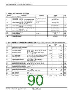
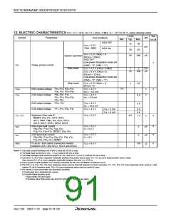
12. ELECTRIC CHARACTERISTICS (VCC = 5 V ± 10 %, VSS = 0 V, f(XIN) = 8 MHz, T
a
= –10 °C to 70 °C, unless otherwise noted)
Limits
Unit
Test
Symbol
Parametear
Test conditions
Min.
Typ.
Max.
circuit
OSD OFF
OSD ON
15
30
VCC = 5.5V,
f(XIN) = 8MHz
mA
30
60
45
VCC = 5.5V, f(XIN) = 0,
f(XCIN) = 32kHz,
µA
200
System operation
Wait mode
OSD OFF
Low-power dissipation mode set
1
2
3
Power source current
ICC
(CM5 = “0”, CM6 = “1”)
VCC = 5.5 V, f(XIN) = 8 MHz
mA
µA
1
25
2
100
VCC = 5.5 V, f(XIN) = 0,
f(XCIN) = 32 kHz,
Low-power dissipation mode set
(CM5 = “0”, CM6 = “1”)
Stop mode
VCC = 5.5V, f(XIN) = 0,
f(XCIN) = 0
1
10
2.4
HIGH output voltage P10–P16, P20–P27,
P30, P31, P52–P55,
VCC = 4.5 V
IOH = –0.5 mA
VOH
VOL
V
V
LOW output voltage P00–P07, P10,
P15, P16, P20–P23,
VCC = 4.5 V
IOL = 0.5 mA
0.4
3.0
P52–P55
LOW output voltage P24– P27
VCC = 4.5 V
IOL = 10.0 mA
LOW output voltage P11–P14, P30, P32
VCC = 4.5 V
VCC = 5.0 V
IOL = 3 mA
IOL = 6 mA
0.4
0.6
1.3
Hysteresis (See note 6)
0.5
VT+ –VT–
V
____________
RESET, P50, P51, INT1, INT2,
INT3, TIM2, TIM3, SIN, SCLK, SCL1,
SCL2, SCL3, SDA1, SDA2, SDA3
HIGH input leak current
4
4
5
VCC = 5.5 V
VI = 5.5 V
µA
µA
5
5
IIZH
IIZL
P00–P07, P10–P16, P20–P27,
P30, P31,P35–P37, _R__E___S__E___T_, P50, P51,
LOW input leak current
VCC = 5.5 V
VI = 0 V
P00–P07, P10–P16, P20–P27, P30, P31,
P35–P37, P50, P51, R___E__S___E__T__
2
RBS
I C-BUS • BUS switch connection resistor
130
Ω
VCC = 4.5 V
(between SCL1 and SCL2, SDA1 and SDA2)
Notes 1: The total current that flows out of the IC must be 20 mA or less.
2: The total input current to IC (IOL1 + IOL2) must be 30 mA or less.
3: The total average input current for ports P24–P27 and AVCC–VSS to IC must be 20 mA or less.
4: Connect 0.1 µF or more capacitor externally between the power source pins VCC–VSS so as to reduce power source noise.
Also connect 0.1 µF or more capacitor externally between the pins VCC–CNVSS.
5: Use a quartz-crystal oscillator or a ceramic resonator for the CPU oscillation circuit(XIN,XOUT).
6: P06, P07, P16, P23, P24, P25 have hysteresis when used as interrupt input pins or timer input pins. P11–P14, P30, P31 have hysteresis when used as multi-
master I2C-BUS interface ports. P20–P22 have hysteresis when used as serial I/O pins.
7: Pin names in each parameter are described as below.
(1) Dedicated pins: dedicated pin names.
(2) Double-/triple-function ports
• Same limits: I/O port name.
• Functions other than ports vary from I/O port limits : function pin name.
Rev.1.00 2003.11.25 page 91 of 128

 RENESAS [ RENESAS TECHNOLOGY CORP ]