M37161M8/MA/MF-XXXSP/FP,M37161EFSP/FP
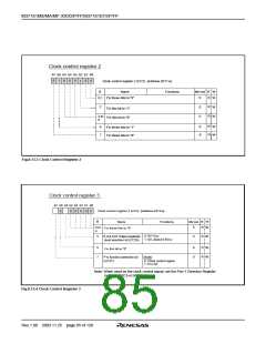
Clock control register 2
b7 b6 b5 b4 b3 b2 b1 b0
0
1
0
0
0
0
0
1
Clock control register 2 (CC2) [Address 021116]
B
Name
Functions
After reset
W
W
R
R
0
Fix these bits to "0"
0,1
2
R
R
0
0
W
W
Fix this bit to "1"
Fix this bit to "0"
3 to
5
R
R
0
0
W
W
6
7
Fix these bits to "1"
Fix these bits to "0"
Fig.8.13.3 Clock Control Register 2
Clock control register 3
b7 b6 b5 b4 b3 b2 b1 b0
Clock control register 3 (CC3) [Address 021216
]
0
0
0
0
0 0
B
Name
Functions
After reset
W
R
R
0
0 to
4
W
Fix these bits to "0"
0: 0V–VCC
1: 0V–About 0.6VCC
5
R
R,G,B,OUT Output amplitude
level selection bit (CC35)
0
W
6
7
R
R
0
0
W
W
Fix this bit to "0"
P10
function-selection bit
(Note)
(CC37)
0: Clock control signal
1: P10 I/O
Note: When used as the clock control signal, set the Port 1 Direction Register
(address 00C316) bit 0 to 1.
Fig.8.13.4 Clock Control Register 3
Rev.1.00 2003.11.25 page 85 of 128

 RENESAS [ RENESAS TECHNOLOGY CORP ]