M37161M8/MA/MF-XXXSP/FP,M37161EFSP/FP
8.13 CLOCK GENERATING CIRCUIT
(3) Low-speed Mode
This microcomputer has 2 built-in oscillation circuits. An oscillation
circuit can be formed by connecting a resonator between XIN and
XOUT (XCIN and XCOUT). Use the circuit constants in accordance with
the resonator manufacturer’s recommended values. No external re-
sistor is needed between XIN and XOUT since a feed-back resistor
exists on-chip. However, an external feed-back resistor is needed
between XCIN and XCOUT. To supply a clock signal externally, input it
to the XIN (XCIN) pin and make the XOUT (XCOUT) pin open. When not
using XCIN clock, connect the XCIN to VSS and make the XCOUT pin
open.
If the internal clock is generated from the sub-clock (XCIN), a low
power consumption operation can be realized by stopping only the
main clock XIN. To stop the main clock, set bit 6 (CM6) of the CPU
mode register (00FB16) to “1.” When the main clock XIN is restarted,
the program must allow enough time for oscillation to stabilize.
Note that in the low-power-consumption mode the XCIN-XCOUT
drivability can be reduced, allowing even lower power consumption.
To reduce the XCIN-XCOUT drivability, clear bit 5 (CM5) of the CPU
mode register (00FB16) to “0.” At reset, this bit is set to “1” and strong
drivability is selected to help the oscillation to start. When executing
an STP instruction, set this bit to “1” by software before initiating the
instruction.
After reset has completed, the internal clock φ is half the frequency of
XIN. Immediately after poweron, both the XIN and XCIN clock start
oscillating. To set the internal clock φ to low-speed operation mode,
set bit 7 of the CPU mode register to “1.”
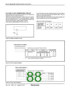
Microcomputer
8.13.1 OSCILLATION CONTROL
(1) Stop Mode
X
CIN
X
COUT
X
IN
XOUT
FILT
The built-in clock generating circuit is shown in Figure 120. When the
STP instruction is executed, the internal clock f stops at HIGH. At the
same time, timers 3 and 4 are connected by hardware and “FF16” is
set in timer 3 and “0716” is set in timer 4. Select f(XIN)/16 or f(XCIN)/
16 as the timer 3 count source (set both bit 0 of timer mode register
2 and bit 6 at address 00C716 to “0” before the execution of the STP
instruction). Moreover, set the timer 3 and timer 4 interrupt enable
bits to disabled (“0”) before execution of the STP instruction. The
oscillator restarts when an external interrupt is accepted. However,
the internal clock f keeps its HIGH level until timer 4 overflows, allow-
ing time for oscillation stabilization when a ceramic resonator or a
quartz-crystal oscillator is used.
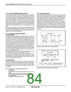
R
f
R
d
0.01µF
C1
CCIN
C
COUT
CIN
COUT
Fig.8.13.1 Ceramic Resonator Circuit Example
By settimg bit 7 of timer return setting register (address 00CC16) to
“1, ” an arbitrarary value can be set to timer 3 and timer 4.
Bit 7 of clock control register 3 (address 020216) can switch Port P10
pin and the CLKCONT. When CLKCONT pin is selected, “H” is output
normally. When an extenal interrupt is recieved in the STP state, the
CLKCONT pin goes back to “H” output.
Microcomputer
X
CIN
X
COUT
X
IN
XOUT
Open
Open
External oscillation
circuit or external
pulse
External oscillation
circuit
(2) Wait Mode
When the WIT instruction is executed, the internal clock φ stops in
the HIGH level but the oscillator continues running. This wait state is
released at reset or when an interrupt is accepted (See note). Since
the oscillator does not stop, the next instruction can be executed
immediately.
Vcc
Vss
Vcc
Vss
Fig.8.13.2 External Clock Input Circuit Example
Note: In the wait mode, the following interrupts are invalid.
• VSYNC interrupt
• OSD interrupt
• All timer interrupts using external clock input from port pin as count
source
• All timer interrupts using f(XIN)/2 or f(XCIN)/2 as count source
• All timer interrupts using f(XIN)/4096 or f(XCIN)/4096 as count source
• f(XIN)/4096 interrupt
• Multi-master I2C-BUS interface interrupt
Rev.1.00 2003.11.25 page 84 of 128

 RENESAS [ RENESAS TECHNOLOGY CORP ]