M37161M8/MA/MF-XXXSP/FP,M37161EFSP/FP
2
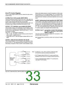
8.6.4 I C Control Register
address and address data as a result of comparison or when a gen-
2
2
The I C control register (address 00F916) controls the data commu-
eral call (refer to “8.6.5 I C Status Register,” bit 1) is received, trans-
nication format.
mission processing can be performed. When this bit is set to “1,” the
free data format is selected, so that slave addresses are not recog-
nized.
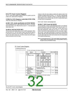
(1) Bits 0 to 2: bit counter (BC0–BC2)
These bits decide the number of bits for the next 1-byte data to be
transmitted. An interrupt request signal occurs immediately after the
number of bits specified with these bits are transmitted.
(4) Bit 5: addressing format selection bit (10BIT SAD)
This bit selects a slave address specification format. When this bit is
set to “0,” the 7-bit addressing format is selected. In this case, only
When a START condition is received, these bits become “0002” and
the address data is always transmitted and received in 8 bits.
2
the high-order 7 bits (slave address) of the I C address register (ad-
dress 00F716) are compared with address data. When this bit is set
to “1,” the 10-bit addressing format is selected and all the bits of the
2
(2) Bit 3: I C interface use enable bit (ESO)
2
2
This bit enables usage of the multimaster I C BUS interface. When
I C address register are compared with the address data.
this bit is set to “0,” interface is in the disabled status, so the SDA and
the SCL become high-impedance. When the bit is set to “1,” use of
the interface is enabled.
(5) Bits 6 and 7: connection control bits between
I2C-BUS interface and ports
(BSEL0, BSEL1)
When ESO = “0,” the following is performed.
2
• PIN = “1,” BB = “0” and AL = “0” are set (they are bits of the I C
These bits control the connection between SCL and ports or SDA
status register at address 00F816 ).
and ports (refer to Figure 8.6.5).
2
• Writing data to the I C data shift register (address 00F616) is dis-
Note: To connect with SCL3 and SDA3, set bits 2 and 3 of the port P3 register
abled.
(00C616) .
(3) Bit 4: data format selection bit (ALS)
This bit decides whether or not to recognize slave addresses. When
this bit is set to “0,” the addressing format is selected, so that ad-
dress data is recognized. When a match is found between a slave
“0”
“1” BSEL20
Notes • The paths SCL1, SCL2, SDA1, and SDA2, as well as the paths
SCL3 and SDA3 cannot be connected at the same time.
SCL3/P3
1
“1”
BSEL21
“0”
“0”
“1”
BSEL0
BSEL1
SCL1/P1
1
SCL
• Port P3 Register (address 00C616) bit 3 is used to control the pin
“0”
“1”
connections of SCL3/P31 and SCL1/P11 and those of SDA3/P30 and SDA1/P13.
SCL2/P1
2
Multi-master
“0”
“1”
BSEL20
I2C-BUS
interface
• Set the corresponding direction register to "1" to use the port as
multi-master I2C-BUS interface.
SDA3/P3
0
“1”
BSEL21
“0”
“0”
“1” BSEL0
SDA1/P1
3
4
SDA
“0”
BSEL1
“1”
SDA2/P1
Fig. 8.6.5 Connection Port Control by BSEL0 and BSEL1
Rev.1.00 2003.11.25 page 33 of 128

 RENESAS [ RENESAS TECHNOLOGY CORP ]