M37161M8/MA/MF-XXXSP/FP,M37161EFSP/FP
2
2
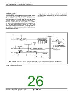
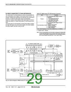
8.6 MULTI-MASTER I C-BUS INTERFACE
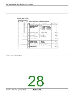
Table 8.6.1 Multi-master I C-BUS Interface Functions
2
The multi-master I C-BUS interface is a serial communications cir-
Item
Function
2
cuit, conforming to the Philips I C-BUS data transfer format. This
2
In conformity with Philips I C-BUS
standard:
10-bit addressing format
7-bit addressing format
High-speed clock mode
Standard clock mode
interface, offering both arbitration lost detection and synchronous
functions, is useful for multi-master serial communications.
Format
2
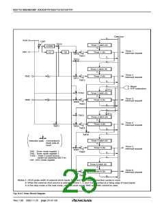
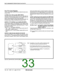
Figure 8.6.1 shows a block diagram of the multi-master I C-BUS in-
2
terface and Table 8.6.1 shows multi-master I C-BUS interface func-
2
tions.
In conformity with Philips I C-BUS
standard:
2
This multi-master I C-BUS interface consists of the address register,
Master transmission
Master reception
Slave transmission
Slave reception
the data shift register, the clock control register, the control register,
the status register and other control circuits.
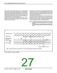
Communication mode
SCL clock frequency 16.1 kHz to 400 kHz (φ = at 4 MHz)
φ : System clock = f(XIN)/2
Note : We are not responsible for any third party’s infringement of patent rights
or other rights attributable to the use of the control function (bits 6 and 7
of the I2C control register at address 00F916) for connections between
the I2C-BUS interface and ports (SCL1, SCL2, SDA1, SDA2).
I2C address register (S0D)
b7
b0
Interrupt
generating
circuit
Interrupt
request signal
(IICIRQ)
SAD6 SAD5 SAD4 SAD3 SAD2 SAD1 SAD0 RBW
Address comparator
Serial
data
(SDA)
Noise
elimination
circuit
Data
control
circuit
b7
b0
I2C data shift register
b7
b0
S0
AL AAS AD0 LRB
I2C control register (S1D)
MST TRX BB PIN
I2C status
register (S1)
AL
circuit
Internal data bus
BB
circuit
Noise
elimination
circuit
Serial
clock
(SCL)
Clock
control
circuit
b7
b0
b7
b0
FAST
MODE
10BIT
ACK
BIT
BSEL1 BSEL0
ALS
CCR4 CCR3 CCR2 CCR1 CCR0
ACK
ESO BC2 BC1 BC0
SAD
I2C control register (S1D)
System clock (φ)
I2C clock control register (S2)
Clock division
Bit counter
2
Fig. 8.6.1 Block Diagram of Multi-master I C-BUS Interface
Rev.1.00 2003.11.25 page 29 of 128

 RENESAS [ RENESAS TECHNOLOGY CORP ]