M37161M8/MA/MF-XXXSP/FP,M37161EFSP/FP
2
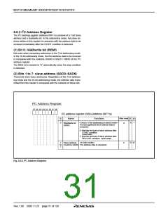
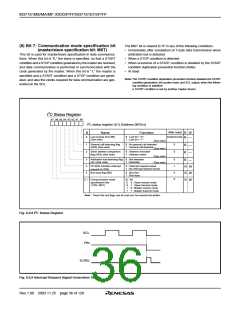
8.6.3 I C Clock Control Register
However, when the slave address matches the address data in the
reception of address data at ACK BIT = “0,” the SDA is automatically
goes to LOW (ACK is returned). If there is a mismatch between the
slave address and the address data, the SDA is automatically goes
to HIGH (ACK is not returned).
2
The I C clock control register (address 00FA16) is used to set ACK
control, SCL mode and SCL frequency.
(1) Bits 0 to 4: SCL frequency control bits (CCR0–CCR4)
These bits control the SCL frequency.
✽ACK clock: Clock for acknowledgement
(2) Bit 5: SCL mode specification bit (FAST MODE)
This bit specifies the SCL mode. When this bit is set to “0,” the stan-
dard clock mode is set. When the bit is set to “1,” the high-speed
clock mode is set.
(4) Bit 7: ACK clock bit (ACK)
This bit specifies a mode of acknowledgment which is an acknowl-
edgment response of data transmission. When this bit is set to “0,”
the no ACK clock mode is set. In this case, no ACK clock occurs
after data transmission. When the bit is set to “1,” the ACK clock
mode is set and the master generates an ACK clock upon comple-
tion of each 1-byte data transmission.The device for transmitting
address data and control data releases the SDA at the occurrence of
an ACK clock (make SDA HIGH) and receives the ACK bit generated
by the data receiving device.
(3) Bit 6: ACK bit (ACK BIT)
✽
This bit sets the SDA status when an ACK clock is generated. When
this bit is set to “0,” the ACK return mode is set and SDA goes to
LOW at the occurrence of an ACK clock. When the bit is set to “1,”
the ACK non-return mode is set. The SDA is held in the HIGH status
at the occurrence of an ACK clock.
Note: Do not write data into the I2C clock control register during transmission.
If data is written during transmission, the I2C clock generator is reset, so
that data cannot be transmitted normally.
2
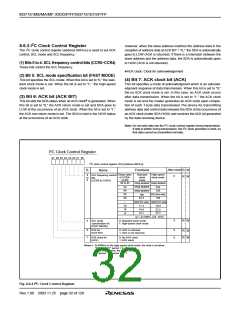
I C Clock Control Register
b7 b6 b5 b4 b3 b2 b1 b0
2
I C clock control register (S2) [Address 00FA16
]
After reset
0
B
Functions
R W
R W
Name
Setup value
of CCR4–
CCR0
Standard
clock
mode
High speed
clock mode
0
to
4
SCL frequency control
bits
(CCR0 to CCR4)
Setup disabled Setup disabled
00 to 02
Setup disabled
333
03
04
05
06
Setup disabled
250
400 (See note)
166
100
83.3
500/CCR value 1000/CCR value
17.2
16.6
16.1
34.5
33.3
32.3
1D
1E
1F
(φ = at 4 MHz, unit : kHz)
0
5
SCL mode
specification bit
(FAST MODE)
0: Standard clock mode
1: High-speed clock mode
R W
6
7
ACK bit
(ACK BIT)
0: ACK is returned.
1: ACK is not returned.
0
0
R W
R W
ACK clock bit
(ACK)
0: No ACK clock
1: ACK clock
Notes 1. At 400kHz in the high-speed clock mode, the duty is as below .
“0” period : “1” period = 3 : 2
In the other cases, the duty is as below.
“0” period : “1” period = 1 : 1
2
Fig. 8.6.4 I C Clock Control Register
Rev.1.00 2003.11.25 page 32 of 128

 RENESAS [ RENESAS TECHNOLOGY CORP ]