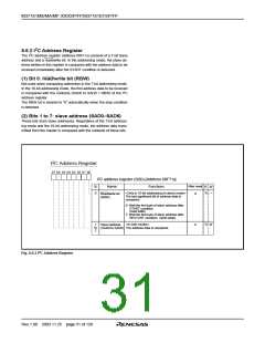
M37161M8/MA/MF-XXXSP/FP,M37161EFSP/FP
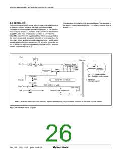
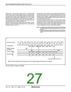
Internal clock : The serial I/O counter is set to “7” during the write
cycle into the serial I/O register (address 00EA16), and the transfer
clock goes HIGH forcibly. At each falling edge of the transfer clock
after the write cycle, serial data is output from the SOUT pin. Transfer
direction can be selected by bit 5 of the serial I/O mode register. At
each rising edge of the transfer clock, data is input from the SIN pin
and data in the serial I/O register is shifted 1 bit.
External clock : The an external clock is selected as the clock source,
the interrupt request is set to “1” after the transfer clock has been
counted 8 counts. However, transfer operation does not stop, so the
clock should be controlled externally. Use the external clock of 1 MHz
or less with a duty cycle of 50%.
The serial I/O timing is shown in Figure 8.5.2. When using an exter-
nal clock for transfer, the external clock must be held at HIGH for
initializing the serial I/O counter. When switching between an inter-
nal clock and an external clock, do not switch during transfer. Also,
be sure to initialize the serial I/O counter after switching.
After the transfer clock has counted 8 times, the serial I/O counter
becomes “0” and the transfer clock stops at HIGH. At this time the
interrupt request bit is set to “1.”
Notes 1: On programming, note that the serial I/O counter is set by writing to
the serial I/O register with the bit managing instructions, such as SEB
and CLB.
2: When an external clock is used as the synchronous clock, write trans-
mit data to the serial I/O register when the transfer clock input level is
HIGH.
Synchronous clock
Transfer clock
Serial I/O register
write signal
(Note)
Serial I/O output
D0
D1
D2
D3
D4
D5
D6
D7
SOUT
Serial I/O input
S
IN
Interrupt request bit is set to “1”
Note : When an internal clock is selected, the SOUT pin is at high-impedance after transfer is completed.
Fig. 8.5.2 Serial I/O Timing (for LSB first)
Rev.1.00 2003.11.25 page 27 of 128

 RENESAS [ RENESAS TECHNOLOGY CORP ]