M37161M8/MA/MF-XXXSP/FP,M37161EFSP/FP
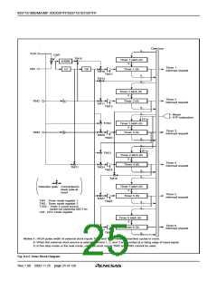
Data bus
8
X
CIN
CM7
TM15
Timer 1 latch (8)
8
1/4096
1/2
Timer 1
interrupt request
XIN
1/8
Timer 1 (8)
TM10
TM14
TM12
8
8
Timer 2 latch (8)
8
Timer 2
interrupt request
TIM2
Timer 2 (8)
TM11
TM13
8
8
Reset
STP instruction
FF16
T3SC
Timer 3 latch (8)
8
Timer 3
interrupt request
Timer 3 (8)
TIM3
TM20
TM22
8
8
0716
TM21
Timer 4 latch (8)
8
Timer 4
interrupt request
Timer 4 (8)
TM21
TM24
TM23
8
8
TM16
Timer 5 latch (8)
8
Selection gate: Connected to
black side at
reset
Timer 5
interrupt request
Timer 5 (8)
TM27
TM25
TM1 : Timer mode register 1
TM2 : Timer mode register 2
T3SC : Timer 3 count source
8
8
switch bit (address 00C716
)
CM : CPU mode register
Timer 6 latch (8)
8
Timer 6
interrupt request
Timer 6 (8)
8
TM17
TM26
Notes 1: HIGH pulse width of external clock inputs TIM2 and TIM3 needs 4 machine cycles or more.
2: When the external clock source is selected, timers 1, 2, and 3 are counted at a rising edge of input signal.
3: In the stop mode or the wait mode, external clock inputs TIM2 and TIM3 cannot be used.
Fig. 8.4.5 Timer Block Diagram
Rev.1.00 2003.11.25 page 25 of 128

 RENESAS [ RENESAS TECHNOLOGY CORP ]