M37161M8/MA/MF-XXXSP/FP,M37161EFSP/FP
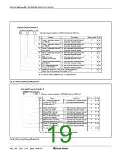
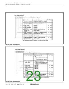
Timer Mode Register 1
b7b6 b5b4b3 b2b1b0
Timer mode register 1 (TM1) [Address 00F4 16
]
After reset
0
B
0
Name
Functions
R
R
W
W
0: f(XIN)/16 or f(XCIN)/16 (See note)
1: Count source selected by bit 5 of TM1
Timer 1 count source
selection bit 1 (TM10)
0: Count source selected by bit 4 of TM1
1: External clock from TIM2 pin
0
R
W
1
Timer 2 count source
selection bit 1 (TM11)
Timer 1 count
stop bit (TM12)
2
3
4
0: Count start
1: Count stop
0
0
0
R
R
R
W
W
W
Timer 2 count stop
bit (TM13)
0: Count start
1: Count stop
Timer 2 count source
selection bit 2
(TM14)
0: f(XIN)/16 or f(XCIN)/16 (See note)
1: Timer 1 overflow
5
Timer 1 count source
selection bit 2 (TM15)
0: f(XIN)/4096 or f(XCIN)/4096 (See note)
1: External clock from TIM2 pin
0
R
W
6
7
Timer 5 count source
selection bit 2 (TM16)
0: Timer 2 overflow
1: Timer 4 overflow
0
0
R
R
W
W
Timer 6 internal count 0: f(XIN)/16 or f(XCIN)/16 (See note)
source selection bit
(TM17)
1: Timer 5 overflow
Note: Either f(XIN) or f(XCIN) is selected by bit 7 of the CPU mode register.
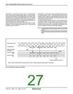
Fig. 8.4.1 Timer Mode Register 1
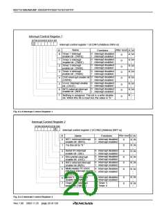
Timer Mode Register 2
b7b6 b5b4b3 b2b1b0
Timer mode register 2 (TM2) [Address 00F516
]
After reset
0
B
0
Name
Functions
R
W
W
Timer 3 count source
selection bit (TM20)
R
(b6 at address 00C716
)
b0
0
1
0
1
0 : f(XIN)/16 or f(XCIN)/16 (See note)
0 : f(XCIN
)
1 :
1 :
External clock from TIM3 pin
b4 b1
1, 4
Timer 4 count source
selection bits
(TM21, TM24)
0
R
W
0
0
1
1
0 : Timer 3 overflow signal
1 : f(XIN)/16 or f(XCIN)/16 (See note)
0 : f(XIN)/2 or f(XCIN)/2 (See note)
1 : f(XCIN
)
Timer 3 count
stop bit (TM22)
2
3
0: Count start
1: Count stop
0
0
R
R
W
W
Timer 4 count stop bit
(TM23)
0: Count start
1: Count stop
Timer 5 count stop bit
(TM25)
5
6
0: Count start
1: Count stop
0
0
R
R
W
W
Timer 6 count stop bit
(TM26)
0: Count start
1: Count stop
Timer 5 count source
selection bit 1
(TM27)
7
0: f(XIN)/16 or f(XCIN)/16 (See note)
1: Count source selected by bit 6
of TM1
0
R
W
Note: Either f(XIN) or f(XCIN) is selected by bit 7 of the CPU mode register.
Fig. 8.4.2 Timer Mode Register 2
Rev.1.00 2003.11.25 page 23 of 128

 RENESAS [ RENESAS TECHNOLOGY CORP ]