M37161M8/MA/MF-XXXSP/FP,M37161EFSP/FP
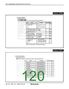
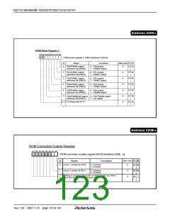
Address 00FA16
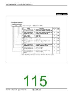
2
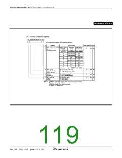
I C Clock Control Register
b7 b6 b5 b4 b3 b2 b1 b0
2
I C clock control register (S2) [Address 00FA16
]
After reset
0
B
Functions
R W
R W
Name
Setup value
of CCR4–
CCR0
Standard
clock
mode
High speed
clock mode
0
to
4
SCL frequency control
bits
(CCR0 to CCR4)
Setup disabled Setup disabled
00 to 02
Setup disabled
333
03
04
05
06
Setup disabled
250
400 (See note)
166
100
83.3
500/CCR value 1000/CCR value
17.2
16.6
16.1
34.5
33.3
32.3
1D
1E
1F
(φ = at 4 MHz, unit : kHz)
0
5
SCL mode
specification bit
(FAST MODE)
0: Standard clock mode
1: High-speed clock mode
R W
6
7
ACK bit
(ACK BIT)
0: ACK is returned.
1: ACK is not returned.
0
0
R W
R W
ACK clock bit
(ACK)
0: No ACK clock
1: ACK clock
Notes 1. At 400kHz in the high-speed clock mode, the duty is as below .
“0” period : “1” period = 3 : 2
In the other cases, the duty is as below.
“0” period : “1” period = 1 : 1
Rev.1.00 2003.11.25 page 119 of 128

 RENESAS [ RENESAS TECHNOLOGY CORP ]