M37161M8/MA/MF-XXXSP/FP,M37161EFSP/FP
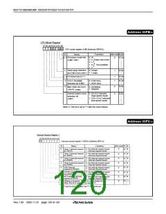
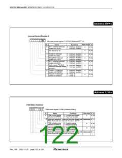
Address 00FF16
Interrupt Control Register 2
b7b6 b5b4b3 b2b1b0
0
Interrupt control register 2 (ICON2) [Address 00FF16
]
After reset
0
B
Name
Functions
R W
R W
INT1 external interrupt
enable bit (IN1E)
0 : Interrupt disabled
1 : Interrupt enabled
0
1
2
3
4
0
R W
Fix this bit to “0.”
Serial I/O interrupt
enable bit (SIE)
0 : Interrupt disabled
1 : Interrupt enabled
0
0
0
R W
R W
R W
0 : Interrupt disabled
1 : Interrupt enabled
0 : Interrupt disabled
1 : Interrupt enabled
f(XIN
)/4096 interrupt
enable bit (CKE)
INT2 external interrupt
enable bit (IN2E)
I2
Multi-master C-BUS
5
0 : Interrupt disabled
1 : Interrupt enabled
0
R W
interface interrupt enable
bit (IICE)
0
0
R W
R W
Timer 5 • 6 interrupt
enable bit (TM56E
Timer 5 • 6 interrupt
switch bit (TM56C)
0 : Interrupt disabled
1 : Interrupt enabled
6
7
)
0 : Timer 5
1 : Timer 6
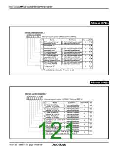
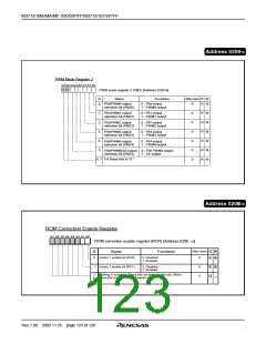
Address 020816
PWM Mode Register 1
b7b6 b5b4b3 b2b1b0
PWM mode register 1 (PM1) [Address 020816
]
After reset
0
B
0
Name
Functions
R W
PWM counts source
selection bit (PM10)
0 : Count source supply
1 : Count source stop
W
R
1, 2
3
—
Nothing is assigned. These bits are write disable bits.
When these bits are read out, the values are “0.”
Indeterminate
0
R
PWM output polarity
selection bit (PM13)
0 : Positive polarity
1 : Negative polarity
R W
R W
4
DA output polarity
selection bit (PM14)
0 : Positive polarity
1 : Negative polarity
0
5
to
7
Nothing is assigned. These bits are write disable bits.
When these bits are read out, the values are “0.”
—
R
Indeterminate
Rev.1.00 2003.11.25 page 122 of 128

 RENESAS [ RENESAS TECHNOLOGY CORP ]