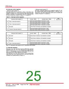
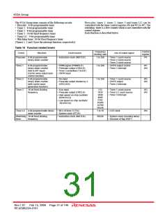
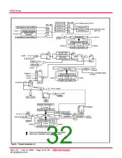
455A Group
(3) Notes on interrupts
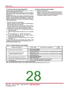
(3) Bit 2 of register I1
When the interrupt valid waveform of the INT pin is
changed with the bit 2 of register I1 in software, be careful
about the following notes.
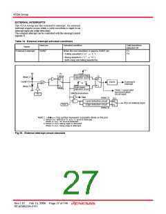
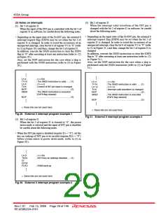
(1) Bit 3 of register I1
When the input of the INT pin is controlled with the bit 3 of
register I1 in software, be careful about the following notes.
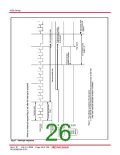
• Depending on the input state of the D5/INT pin, the external 0
interrupt request flag (EXF0) may be set when the bit 2 of
register I1 is changed. In order to avoid the occurrence of an
unexpected interrupt, clear the bit 0 of register V1 to “0” (refer
to (1) in Figure 31.) and then, change the bit 2 of register I1 is
changed.
In addition, execute the SNZ0 instruction to clear the EXF0
flag to “0” after executing at least one instruction (refer to (2)
in Figure 31.).
• Depending on the input state of the D5/INT pin, the external 0
interrupt request flag (EXF0) may be set when the bit 3 of
register I1 is changed. In order to avoid the occurrence of an
unexpected interrupt, clear the bit 0 of register V1 to “0” (refer
to (1) in Figure 29.) and then, change the bit 3 of register I1.
In addition, execute the SNZ0 instruction to clear the EXF0
flag to “0” after executing at least one instruction (refer to (2)
in Figure 29.).
Also, set the NOP instruction for the case when a skip is
performed with the SNZ0 instruction (refer to (3) in Figure
29.).
Also, set the NOP instruction for the case when a skip is
performed with the SNZ0 instruction (refer to (3) in Figure
31.).
•
•
•
•
•
•
LA 4
TV1A
LA 8
TI1A
NOP
SNZ0
; (×××02)
; The SNZ0 instruction is valid ...... (1)
; (1×××2)
; Control of INT pin input is changed
...................................................... (2)
; The SNZ0 instruction is executed
(EXF0 flag cleared)
LA 4
; (×××02)
TV1A
LA 12
TI1A
NOP
SNZ0
; The SNZ0 instruction is valid ......(1)
; (×1××2)
; Interrupt valid waveform is changed
.......................................................(2)
; The SNZ0 instruction is executed
(EXF0 flag cleared)
NOP
...................................................... (3)
•
•
•
NOP
.......................................................(3)
•
•
•
×: these bits are not used here.
×: these bits are not used here.
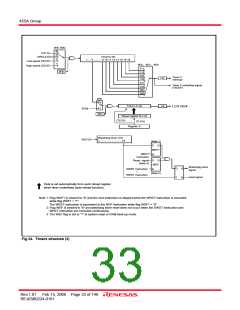
Fig 29. External 0 interrupt program example-1
Fig 31. External 0 interrupt program example-3
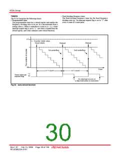
(2) Bit 3 of register I1
When the bit 3 of register I1 is cleared to “0”, the power
down mode is selected and the input of INT pin is disabled,
be careful about the following notes.
• When the INT pin input is disabled (register I13 = “0”), set the
key-on wakeup of INT pin to be invalid (register K20 = “0”)
before system enters to power down mode. (refer to (1) in
Figure 30.).
•
•
•
LA 0
TK2A
DI
; (×××02)
; INT0 key-on wakeup disabled .....(1)
EPOF
POF2
; RAM back-up
•
•
•
×: these bits are not used here.
Fig 30. External 0 interrupt program example-2
Rev.1.01 Feb 15, 2008 Page 29 of 146
REJ03B0224-0101

 RENESAS [ RENESAS TECHNOLOGY CORP ]