455A Group
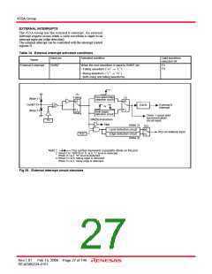
(1) External 0 interrupt request flag (EXF0)
(2) External interrupt control registers
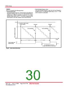
External 0 interrupt request flag (EXF0) is set to “1” when a
valid waveform is input to D5/INT pin.
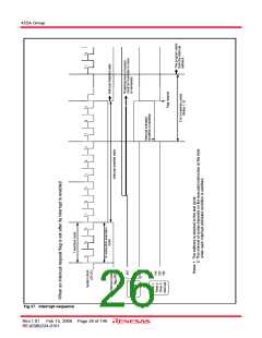
The valid waveforms causing the interrupt must be retained at
their level for 4 clock cycles or more of the system clock (Refer
to Figure 27).
The state of EXF0 flag can be examined with the skip instruction
(SNZ0). Use the interrupt control register V1 to select the
interrupt or the skip instruction. The EXF0 flag is cleared to “0”
when an interrupt occurs or when the next instruction is skipped
with the skip instruction.
(1) Interrupt control register I1
Register I1 controls the valid waveform for the external 0
interrupt. Set the contents of this register through register A
with the TI1A instruction. The TAI1 instruction can be used
to transfer the contents of register I1 to register A.
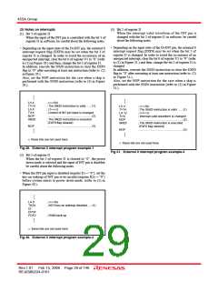
• External 0 interrupt activated condition
External 0 interrupt activated condition is satisfied when a
valid waveform is input to D5/INT pin.
The valid waveform can be selected from rising waveform,
falling waveform or both rising and falling waveforms. An
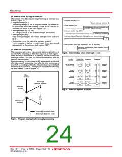
example of how to use the external 0 interrupt is as follows.
(1) Set the bit 3 of register I1 to “1” for the INT pin to be in the
input enabled state.
(2) Select the valid waveform with the bits 1 and 2 of register
I1.
(3) Clear the EXF0 flag to “0” with the SNZ0 instruction.
(4) Set the NOP instruction for the case when a skip is
performed with the SNZ0 instruction.
(5) Set both the external 0 interrupt enable bit (V10) and the
INTE flag to “1.”
The external 0 interrupt is now enabled. Now when a valid
waveform is input to the D5/INT pin, the EXF0 flag is set to “1”
and the external 0 interrupt occurs.
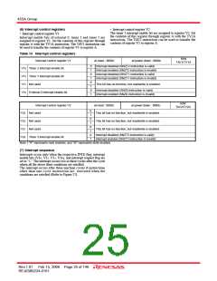
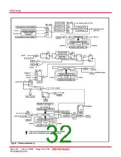
Table 15 External interrupt control register
R/W
at power down : state retained
TAI1/TI1A
Interrupt control register I1
at reset : 00002
INT pin input disabled
0
1
I13 INT pin input control bit (Note 2)
INT pin input enabled
Falling waveform (“L” level of INT pin is recognized with the SNZI0
instruction)/“L” level
0
1
Interrupt valid waveform for INT pin/
I12
return level selection bit (Note 2)
Rising waveform (“H” level of INT pin is recognized with the SNZI0
instruction)/“H” level
0
1
0
1
One-sided edge detected
Both edges detected
I11 INT pin edge detection circuit control bit
INT pin timer 1 count start synchronous cir-
I10
Timer 1 count start synchronous circuit not selected
Timer 1 count start synchronous circuit selected
cuit selection bit
Note 1.“R” represents read enabled, and “W” represents write enabled.
Note 2.When the contents of I12 and I13 are changed, the external interrupt request flag EXF0 may be set.
Rev.1.01 Feb 15, 2008 Page 28 of 146
REJ03B0224-0101

 RENESAS [ RENESAS TECHNOLOGY CORP ]