9.3
Clock Operating Modes
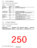
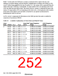
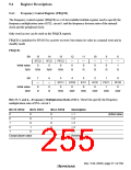
Table 9.3 shows the relationship between the mode control pin (MD2–MD0) combinations and the
clock operating modes. Table 9.4 shows the usable frequency ranges in the clock operating modes.
Table 9.3 Clock Operating Modes
Pin Values
Clock I/O
PLL2
PLL1 Divider 1 Divider 2 CKIO
Mode MD2 MD1 MD0 Source Output On/Off On/Off Input
Input
Frequency
0
1
2
0
0
0
1
0
0
1
1
0
EXTAL CKIO
EXTAL CKIO
On,
multi-
plication
ratio: 1
On
On
On
On
PLL1
output
PLL1
(EXTAL)
1
On,
multi-
plication
ratio: 4
PLL1
output
PLL1
PLL1
PLL1
(EXTAL) × 4
(Crystal) × 4
(CKIO)
0
1
Crystal CKIO
oscillator
On,
multi-
plication
ratio: 4
PLL1
output
7
CKIO
—
Off
PLL1
output
—
Except above
value
Reserved
Mode 0: An external clock is input from the EXTAL pin and undergoes waveform shaping by
PLL circuit 2 before being supplied inside the chip. PLL circuit 1 is constantly on. An input clock
frequency of 25 MHz to 66.67 MHz can be used, and the CKIO frequency range is 25 MHz to
66.67 MHz.
Mode 1: An external clock is input from the EXTAL pin and its frequency is multiplied by 4 by
PLL circuit 2 before being supplied inside the chip, allowing a low-frequency external clock to be
used. An input clock frequency of 6.25 MHz to 16.67 MHz can be used, and the CKIO frequency
range is 25 MHz to 66.67 MHz.
Mode 2: The on-chip crystal oscillator operates, with the oscillation frequency being multiplied
by 4 by PLL circuit 2 before being supplied inside the chip, allowing a low crystal frequency to be
used. A crystal oscillation frequency of 6.25 MHz to 16.67 MHz can be used, and the CKIO
frequency range is 25 MHz to 66.67 MHz.
Rev. 5.00, 09/03, page 207 of 760

 RENESAS [ RENESAS TECHNOLOGY CORP ]