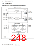
The clock pulse generator blocks function as follows:
1. PLL Circuit 1: PLL circuit 1 doubles, triples, quadruples, sextuples, or leaves unchanged the
input clock frequency from the CKIO pin. The multiplication rate is set by the frequency
control register. When this is done, the phase of the leading edge of the internal clock is
controlled so that it will agree with the phase of the leading edge of the CKIO pin.
2. PLL Circuit 2: PLL circuit 2 leaves unchanged or quadruples the frequency of the crystal
oscillator or the input clock frequency from the EXTAL pin. The multiplication ratio is fixed
by the clock operation mode. The clock operation mode is set by pins MD0, MD1, and MD2.
See table 9.3 for more information on clock operation modes.
3. Crystal Oscillator: This oscillator is used when a crystal oscillator element is connected to the
XTAL and EXTAL pins. It operates according to the clock operating mode setting.
4. Divider 1: Divider 1 generates a clock at the operating frequency used by the internal clock.
The operating frequency can be 1, 1/2, 1/3, 1/4 or 1/6 times the output frequency of PLL
circuit 1, as long as it is not lower than the CKIO pin clock frequency. The division ratio is set
in the frequency control register.
5. Divider 2: Divider 2 generates a clock at the operating frequency used by the peripheral clock.
The operating frequency can be 1, 1/2, 1/3, 1/4 or 1/6 times the output frequency of PLL
circuit 1 or the CKIO pin clock frequency, as long as it is not higher than the CKIO pin clock
frequency. The division ratio is set in the frequency control register.
6. Clock Frequency Control Circuit: The clock frequency control circuit controls the clock
frequency using the MD pins and the frequency control register.
7. Standby Control Circuit: The standby control circuit controls the state of the clock pulse
generator and other modules during clock switching and sleep/standby modes.
8. Frequency Control Register: The frequency control register has control bits assigned for the
following functions: the frequency multiplication ratio of PLL 1, and the frequency division
ratio of the internal clock and the peripheral clock.
9. Standby Control Register: The standby control register has bits for controlling the power-down
modes. See section 8, Power-Down Modes, for more information.
Rev. 5.00, 09/03, page 205 of 760

 RENESAS [ RENESAS TECHNOLOGY CORP ]