21.2.4
Interrupt Source Register (SDINT) (SH7750R Only)
The interrupt source register (SDINT) is a 16-bit register that can be read from and written to by
the CPU.
From the H-UDI pins, the INTREQ bit is set to 1 when a H-UDI interrupt command is set in the
SDIR register (Update-IR). While SDIR is holding a H-UDI interrupt command, the SDINT
register is connected between the TDI and TDO pins of the H-UDI, allowing it to be read as a 32-
bit register. In this case, the upper 16 bits will all be 0, and the lower 16 bits will represent SDINT.
From the CPU, only writing a 0 to the INTREQ bit is possible. While this bit holds a 1, the
interrupt requests continue to be issued, so this bit should always be cleared in the interrupt
handler.
This register is initialized in the Test-Logic-Reset state of 7567 or TAP.
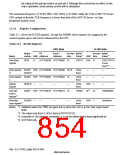
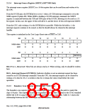
Bit:
15
—
0
14
—
0
13
—
0
12
—
0
11
—
0
10
—
0
9
—
0
8
—
0
Initial value:
R/W:
R
R
R
R
R
R
R
R
Bit:
7
—
0
6
—
0
5
—
0
4
—
0
3
—
0
2
—
0
1
—
0
0
INTREQ
0
Initial value:
R/W:
R
R
R
R
R
R
R
R/W
Bits 15 to 1—Reserved: These bits are always read as 0. When writing, only 0s should be written
here.
Bit 0 Interrupt Request (INTREQ): Indicates whether or not an interrupt request has been
issued by an H-UDI interrupt command. From the CPU, the interrupt request can be cleared by
writing a 0 to this bit. If a 1 is written to this bit, it retains the value it had before the write
operation.
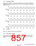
21.2.5
Boundary Scan Register (SDBSR) (SH7750R Only)
The boundary scan register (SDBSR) is a shift register that is placed on the pads to control the
chip’s I/O pins. This register can perform a boundary scan test that conforms to the JTAG standard
(IEEE Std 1149.1) using EXTEST, SAMPLE, and PRELOAD commands. Table 21.3 shows the
relationship between the SH7750R’s pins and the boundary scan register.
Rev. 6.0, 07/02, page 806 of 986

 RENESAS [ RENESAS TECHNOLOGY CORP ]