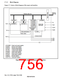
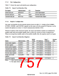
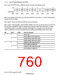
17.2.3 Serial Control Register (SCSCR1)
Bits 1 and 0 of SCSCR1 have a different function in smart card interface mode.
Bit:
7
TIE
0
6
RIE
0
5
TE
0
4
RE
0
3
—
2
—
1
CKE1
0
0
CKE0
0
Initial value:
R/W:
0
0
R/W
R/W
R/W
R/W
R/W
R/W
R/W
R/W
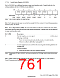
Bits 7 to 4: Operate in the same way as for the normal SCI. See section 15, Serial Communication
Interface (SCI), for details.
Bits 3 and 2—Reserved: Not used with the smart card interface.
Bits 1 and 0—Clock Enable 1 and 0 (CKE1, CKE0): These bits specify the function of the SCK
pin. In smart card interface mode, an internal clock is always used as the clock source. In smart
card interface mode, it is possible to specify a fixed high level or fixed low level for the clock
output, in addition to the usual switching between enabling and disabling of the clock output.
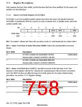
GM
CKE1
CKE0
SCK Pin Function
0
0
0
1
0
1
0
1
0
1
Port I/O pin
Clock output as SCK output pin
Invalid setting: must not be used
Invalid setting: must not be used
Output pin with output fixed low
Clock output as output pin
Output pin with output fixed high
Clock output as output pin
1
0
1
1
Rev. 6.0, 07/02, page 708 of 986

 RENESAS [ RENESAS TECHNOLOGY CORP ]