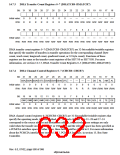
Bit 17—Acknowledge Mode (AM): In dual address mode, selects whether DACK is output in the
data read cycle or write cycle. In single address mode, DACK is always output regardless of the
setting of this bit.
In normal DMA mode, this bit is valid only in CHCR0 and CHCR1. In DDT mode, it is valid in
CHCR0–CHCR7. (DDT mode: 7'$&.) For details of the settings, see the description of the AM
bit in section 14.2.4, DMA Channel Control Registers 0–3 (CHCR0–CHCR3).
Bit 16—Acknowledge Level (AL): Specifies the DACK (acknowledge) signal as active-high or
active-low.
This bit is valid only in CHCR0 and CHCR1 in normal mode, and is invalid in DDT mode. For
details of the settings, see the description of the AL bit in section 14.2.4, DMA Channel Control
Registers 0–3 (CHCR0–CHCR3).
Bits 15 and 14—Destination Address Mode 1 and 0 (DM1, DM0): These bits specify
incrementing/decrementing of the DMA transfer destination address. The specification of these
bits is ignored when data is transferred from external memory to an external device in single
address mode. For details of the settings, see the description of the DM1 and DM0 bits in section
14.2.4, DMA Channel Control Registers 0–3 (CHCR0–CHCR3).
Bits 13 and 12—Source Address Mode 1 and 0 (SM1, SM0): These bits specify
incrementing/decrementing of the DMA transfer source address. The specification of these bits is
ignored when data is transferred from an external device to external memory in single address
mode. For details of the settings, see the description of the SM1 and SM0 bits in section 14.2.4,
DMA Channel Control Registers 0–3 (CHCR0–CHCR3).
Bits 11 to 8—Resource Select 3 to 0 (RS3–RS0): These bits specify the transfer request source.
For details of the settings, see the description of the RS3–RS0 bits in section 14.2.4, DMA
Channel Control Registers 0–3 (CHCR0–CHCR3).
Bit 7—Transmit Mode (TM): Specifies the bus mode for transfer. For details of the settings, see
the description of the TM bit in section 14.2.4, DMA Channel Control Registers 0–3 (CHCR0–
CHCR3).
Bits 6 to 4—Transmit Size 2 to 0 (TS2–TS0): These bits specify the transfer data size (access
size). For details of the settings, see the description of the TS2–TS0 bits in section 14.2.4, DMA
Channel Control Registers 0–3 (CHCR0–CHCR3).
Bit 3 Request Queue Clear (QCL): Writing a 1 to this bit clears the request queues of the
corresponding channel as well as any external requests that have already been accepted. This bit is
only functional when DMAOR.DDT = 1 and DMAOR.DBL = 1.
Rev. 6.0, 07/02, page 582 of 986

 RENESAS [ RENESAS TECHNOLOGY CORP ]