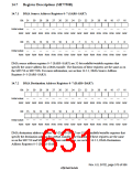
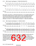
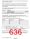
14.7.3
DMA Transfer Count Registers 0–7 (DMATCR0–DMATCR7)
Bit: 31
30
29
28
27
26
25
24
23
22
21
20
19
—
18
—
17
—
16
—
Initial value:
R/W:
0
0
0
0
0
0
0
0
—
—
—
—
R
R
R
R
R
R
R
R
R/W R/W R/W R/W R/W R/W R/W R/W
Bit: 15
14
13
12
11
10
9
8
7
6
5
4
3
2
1
0
Initial value:
—
—
—
—
—
—
—
—
—
—
—
—
—
—
—
—
R/W: R/W R/W R/W R/W R/W R/W R/W R/W R/W R/W R/W R/W R/W R/W R/W R/W
DMA transfer count registers 0–7 (DMATCR0–DMATCR7) are 32-bit readable/writable registers
that specify the number of transfers in transfer operations for the corresponding channel (byte
count, word count, longword count, quadword count, or 32-byte count). Functions of these
registers are the same as the transfer-count registers of the SH7750 or SH7750S. For more
information, see section 14.2.3, DMA Transfer Count Registers 0–3 (DMATCR0–DMATCR3).
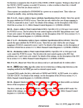
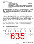
14.7.4 DMA Channel Control Registers 0–7 (CHCR0–CHCR7)
Bit: 31
30
29
28
27
26
25
24
23
—
0
22
—
0
21
—
0
20
—
0
19
18
17
16
SSA2 SSA1 SSA0 STC DSA2DSA1DSA0 DTC
DS RL AM AL
Initial value:
0
0
0
0
0
0
0
0
0
0
0
0
R/W: R/W R/W R/W R/W R/W R/W R/W R/W
R
R
R
R
R/W (R/W) R/W (R/W)
Bit: 15
14
13
12
11
10
9
8
7
6
5
4
3
2
1
0
DM1 DM0 SM1 SM0 RS3 RS2 RS1 RS0 TM TS2 TS1 TS0 QCL IE
TE DE
Initial value:
0
0
0
0
0
0
0
0
0
0
0
0
0
0
0
0
R/W: R/W R/W R/W R/W R/W R/W R/W R/W R/W R/W R/W R/W R/(W) R/W R/(W) R/W
DMA channel control registers 0–7(CHCR0–CHCR7) are 32-bit readable/writable registers that
specify the operating mode, transfer method, etc., for each channel. Bits 31–28 and 27–24
correspond to the source address and destination address, respectively; these settings are only
valid when the transfer involves the CS5 or CS6 space and the relevant space has been specified as
a PCMCIA-interface space. In other cases, these bits should be cleared to 0. For more information
about the PCMCIA interface, see section 13.3.7, PCMCIA Interface, in section 13, Bus State
Controller.
Rev. 6.0, 07/02, page 580 of 986

 RENESAS [ RENESAS TECHNOLOGY CORP ]