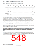
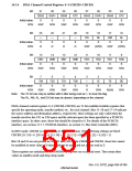
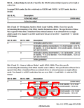
14.2.4 DMA Channel Control Registers 0–3 (CHCR0–CHCR3)
Bit:
31
SSA2
0
30
SSA1
0
29
SSA0
0
28
STC
0
27
DSA2
0
26
DSA1
0
25
DSA0
0
24
DTC
0
Initial value:
R/W:
R/W
R/W
R/W
R/W
R/W
R/W
R/W
R/W
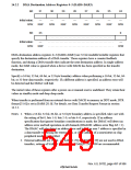
Bit:
23
—
0
22
—
0
21
—
0
20
—
0
19
DS
0
18
RL
17
AM
0
16
AL
Initial value:
R/W:
0
0
R
R
R
R
R/W
(R/W)
R/W
(R/W)
Bit:
15
DM1
0
14
DM0
0
13
SM1
0
12
SM0
0
11
RS3
0
10
RS2
0
9
8
RS1
0
RS0
0
Initial value:
R/W:
R/W
R/W
R/W
R/W
R/W
R/W
R/W
R/W
Bit:
7
TM
0
6
5
4
3
—
0
2
IE
1
TE
0
DE
0
TS2
0
TS1
0
TS0
0
Initial value:
R/W:
0
0
R/W
R/W
R/W
R/W
R
R/W
R/(W)
R/W
Note: The TE bit can only be written with 0 after being read as 1, to clear the flag.
The RL, AM, AL, and DS bits may be absent, depending on the channel.
DMA channel control registers 0–3 (CHCR0–CHCR3) are 32-bit readable/writable registers that
specify the operating mode, transfer method, etc., for each channel. Bits 31–28 and 27–24 indicate
the source address and destination address, respectively; these settings are only valid when the
transfer involves the CS5 or CS6 space and the relevant space has been specified as a PCMCIA
interface space. In other cases, these bits should be cleared to 0. For details of the PCMCIA
interface, see section 13.3.7, PCMCIA Interface, in section 13, Bus State Controller (BSC).
In DDT mode, CHCR0 is set according to the DTR format. (The following settings are fixed:
CHCR0 [31:24] = 0, [18:16] = 0, [15:14] = 01, [13:12] = 01, [2] = 0, [1] = 0, [0] = 1)
Bits 18 and 16 are not present in CHCR2 and CHCR3. In CHCR2 and CHCR3, these bits cannot
be modified (a write value of 0 should always be used) and are always read as 0.
These registers are initialized to H'00000000 by a power-on or manual reset. They retain their
values in standby mode and deep sleep mode.
Rev. 6.0, 07/02, page 499 of 986

 RENESAS [ RENESAS TECHNOLOGY CORP ]