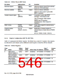
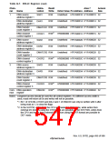
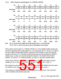
Table 14.3 DMAC Registers (cont)
Chan-
nel
Abbre-
viation
Read/
Write
Area 7
Access
Size
Name
Initial Value P4 Address Address
1
2
3
DMA source
address register 1
R/W
Undefined H'FFA00010 H'1FA00010 32
Undefined H'FFA00014 H'1FA00014 32
Undefined H'FFA00018 H'1FA00018 32
SAR1
DMA destination
address register 1
R/W
DAR1
DMA transfer
count register 1
R/W
DMATCR1
CHCR1
SAR2
1
*
DMA channel
control register 1
R/W
R/W
R/W
H'00000000
Undefined
Undefined
H'1FA0001C 32
H'1FA00020 32
H'1FA00024 32
H'FFA0001C
H'FFA00020
H'FFA00024
DMA source
address register 2
DMA destination
address register 2
DAR2
DMA transfer
count register 2
DMATCR2 R/W
Undefined H'FFA00028 H'1FA00028 32
H'00000000 H'FFA0002C H'1FA0002C 32
Undefined H'FFA00030 H'1FA00030 32
Undefined H'FFA00034 H'1FA00034 32
Undefined H'FFA00038 H'1FA00038 32
H'00000000 H'FFA0003C H'1FA0003C 32
H'00000000 H'FFA00040 H'1FA00040 32
1
*
DMA channel
control register 2
CHCR2
SAR3
R/W
R/W
R/W
DMA source
address register 3
DMA destination
address register 3
DAR3
DMA transfer
count register 3
DMATCR3 R/W
1
1
*
*
DMA channel
control register 3
CHCR3
DMAOR
R/W
R/W
Com- DMA operation
mon register
Notes: Longword access should be used for all control registers. If a different access width is
used, reads will return all 0s and writes will not be possible.
*1 Bit 1 of CHCR0–CHCR3 and bits 2 and 1 of DMAOR can only be written with 0 after
being read as 1, to clear the flags.
*2 In the SH7750, writes from the CPU are masked in DDT mode, while writes from
external I/O devices using the DTR format are possible. In the SH7750S, writes from
the CPU and writes from external I/O devices using the DTR format are possible In
DDT mode.
Rev. 6.0, 07/02, page 495 of 986

 RENESAS [ RENESAS TECHNOLOGY CORP ]