RAS Down Mode: The synchronous DRAM bank function is used to support high-speed accesses
to the same row address. When the RASD bit in MCR is 1, read/write command accesses are
performed using commands without auto-precharge (READ, WRIT). In this case, precharging is
not performed when the access ends. When accessing the same row address in the same bank, it is
possible to issue the READ or WRIT command immediately, without issuing an ACTV command,
in the same way as in the DRAM RAS down state. As synchronous DRAM is internally divided
into two or four banks, it is possible to activate one row address in each bank. If the next access is
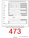
to a different row address, a PRE command is first issued to precharge the relevant bank, then
when precharging is completed, the access is performed by issuing an ACTV command followed
by a READ or WRIT command. If this is followed by an access to a different row address, the
access time will be longer because of the precharging performed after the access request is issued.
In a write, when auto-precharge is performed, a command cannot be issued for a period of Trwl +
Tpc cycles after issuance of the WRIT command. When RAS down mode is used, READ or
WRIT commands can be issued successively if the row address is the same. The number of cycles
can thus be reduced by Trwl + Tpc cycles for each write. The number of cycles between issuance
of the precharge command and the row address strobe command is determined by bits TPC2–
TPC0 in MCR.
There is a limit on tRAS, the time for placing each bank in the active state. If there is no guarantee
that there will not be a cache hit and another row address will be accessed within the period in
which this value is maintained by program execution, it is necessary to set auto-refresh and set the
refresh cycle to no more than the maximum value of tRAS. In this way, it is possible to observe the
restrictions on the maximum active state time for each bank. If auto-refresh is not used, measures
must be taken in the program to ensure that the banks do not remain active for longer than the
prescribed time.
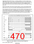
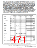
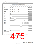
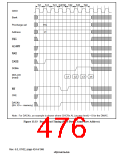
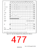
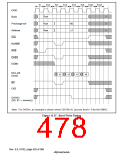
A burst read cycle without auto-precharge is shown in figure 13.32, a burst read cycle for the same
row address in figure 13.33, and a burst read cycle for different row addresses in figure 13.34.
Similarly, a burst write cycle without auto-precharge is shown in figure 13.35, a burst write cycle
for the same row address in figure 13.36, and a burst write cycle for different row addresses in
figure 13.37.
When synchronous DRAM is read, there is a 2-cycle latency for the DMQn signal that performs
the byte specification. As a result, when the READ command is issued in figure 13.32, if the Tc
cycle is executed immediately, the DMQn signal specification for Td1 cycle data output cannot be
carried out. Therefore, the CAS latency should not be set to 1.
When RAS down mode is set, if only accesses to the respective banks in area 3 are considered, as
long as accesses to the same row address continue, the operation starts with the cycle in figure
13.32 or 13.35, followed by repetition of the cycle in figure 13.33 or 13.36. An access to a
different area during this time has no effect. If there is an access to a different row address in the
bank active state, after this is detected the bus cycle in figure 13.34 or 13.37 is executed instead of
Rev. 6.0, 07/02, page 422 of 986

 RENESAS [ RENESAS TECHNOLOGY CORP ]