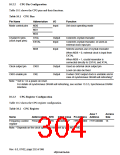
10.3
Clock Operating Modes
Tables 10.3 (1) and 10.3 (2) show the clock operating modes corresponding to various
combinations of mode control pin (MD2–MD0) settings (initial settings such as the frequency
division ratio).
Table 10.4 shows FRQCR settings and internal clock frequencies.
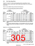
Table 10.3 (1) Clock Operating Modes (SH7750, SH7750S)
External
Frequency
Pin Combination
(vs. Input Clock)
Clock
Operating
Mode
1/2
Frequency
MD2 MD1 MD0 Divider
Peripheral
Module
PLL1 PLL2 Clock Clock Clock
CPU
Bus
FRQCR
Initial Value
0
1
2
3
4
5
0
0
1
0
0
1
0
1
0
1
Off
Off
On
Off
On
Off
On
On
On
On
On
On
On
On
On
On
On
On
6
6
3
6
3
6
3/2
1
3/2
1
H'0E1A
H'0E23
H'0E13
H'0E13
H'0E0A
H'0E0A
1
1/2
1
2
1
3/2
3
3/4
3/2
Notes: 1. Turning on/off of the ½ frequency divider is solely determined by the clock operating
mode.
2. For the ranges of input clock frequency, see the descriptions of the EXTAL clock input
frequency (fEX) and CKIO clock output (fOP) in section 22.3.1, Clock and Control Signal
Timing.
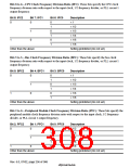
Table 10.3 (2) Clock Operating Modes (SH7750R)
External
Frequency
Pin Combination
(vs. Input Clock)
Clock
Operating
Mode
CPU
PLL2 Clock
Bus
Clock
Peripheral
Module Clock
FRQCR
Initial Value
MD2
MD1
MD0
PLL1
0
1
2
3
4
5
6
0
0
0
1
0
1
0
1
0
On (×12) On
On (×12) On
12
12
6
3
3
H'0E1A
H'0E2C
H'0E13
H'0E13
H'0E0A
H'0E0A
H'0808
3/2
2
3/2
1
1
0
1
On (×6)
On (×12) On
On (×6) On
On (×12) On
Off (×6) Off
On
12
6
4
2
1
3
3/2
3
12
1
6
1/2
1/2
Notes: 1. The multiplication factor of PLL 1 is solely determined by the clock operating mode.
2. For the ranges of input clock frequency, see the descriptions of the EXTAL clock input
frequency (fEX) and CKIO clock output (fOP) in section 22.3.1, Clock and Control Signal
Timing.
Rev. 6.0, 07/02, page 253 of 986

 RENESAS [ RENESAS TECHNOLOGY CORP ]