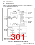
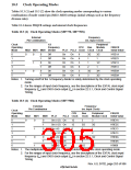
10.2.2 CPG Pin Configuration
Table 10.1 shows the CPG pins and their functions.
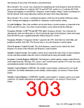
Table 10.1 CPG Pins
Pin Name
Abbreviation
MD0
I/O
Function
Mode control pins
Input
Set clock operating mode
MD1
MD2
Crystal I/O pins
(clock input pins)
XTAL
Output
Input
Connects crystal resonator
EXTAL
Connects crystal resonator, or used as
external clock input pin
MD8
Input
Selects use/non-use of crystal resonator
When MD8 = 0, external clock is input from
EXTAL
When MD8 = 1, crystal resonator is
connected directly to EXTAL and XTAL
Clock output pin
CKIO enable pin
CKIO
CKE
Output
Output
Used as external clock output pin
Level can also be fixed
0 when CKIO output clock is unstable and in
case of synchronous DRAM self-refreshing*
Note: * Set to 1 in a power-on reset.
For details of synchronous DRAM self-refreshing, see section 13.3.5, Synchronous DRAM
Interface.
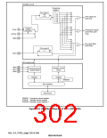
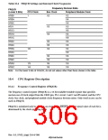
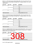
10.2.3 CPG Register Configuration
Table 10.2 shows the CPG register configuration.
Table 10.2 CPG Register
Area 7
Access
Size
Name
Abbreviation R/W
Initial Value P4 Address Address
Frequency control FRQCR
register
R/W
Undefined*
H'FFC00000 H'1FC00000 16
Note: * Depends on the clock operating mode set by pins MD2–MD0.
Rev. 6.0, 07/02, page 252 of 986

 RENESAS [ RENESAS TECHNOLOGY CORP ]