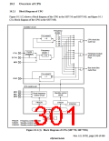
The function of each of the CPG blocks is described below.
PLL Circuit 1: PLL circuit 1 has a function for multiplying the clock frequency from the EXTAL
pin or crystal oscillator by 6 with the SH7750 and SH7750S, and by 6 or 12 with the SH7750R.
Starting and stopping is controlled by a frequency control register setting. Control is performed so
that the internal clock rising edge phase matches the input clock rising edge phase.
PLL Circuit 2: PLL circuit 2 coordinates the phases of the bus clock and the CKIO pin output
clock. Starting and stopping is controlled by a frequency control register setting.
Crystal Oscillator: This is the oscillator circuit used when a crystal resonator is connected to the
XTAL and EXTAL pins. Use of the crystal oscillator can be selected with the MD8 pin.
Frequency Divider 1 (SH7750 and SH7750S only): Frequency divider 1 has a function for
adjusting the clock waveform duty to 50% by halving the input clock frequency when clock input
from the EXTAL pin is supplied internally without using PLL circuit 1.
Frequency Divider 2: Frequency divider 2 generates the CPU clock (Iφ), bus clock (Bφ), and
peripheral module clock (Pφ). The division ratio is set in the frequency control register.
Clock Frequency Control Circuit: The clock frequency control circuit controls the clock
frequency by means of the MD pins and frequency control register.
Standby Control Circuit: The standby control circuit controls the state of the on-chip oscillation
circuits and other modules when the clock is switched and in sleep and standby modes.
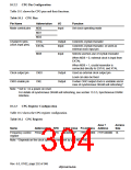
Frequency Control Register (FRQCR): The frequency control register contains control bits for
clock output from the CKIO pin, PLL circuit 1 and 2 on/off control, and the CPU clock, bus clock,
and peripheral module clock frequency division ratios.
Standby Control Register (STBCR): The standby control register contains power save mode
control bits. For further information on the standby control register, see section 9, Power-Down
Modes.
Standby Control Register 2 (STBCR2): Standby control register 2 contains a power save mode
control bit. For further information on standby control register 2, see section 9, Power-Down
Modes.
Rev. 6.0, 07/02, page 251 of 986

 RENESAS [ RENESAS TECHNOLOGY CORP ]