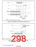
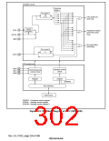
Oscillator circuit
Frequency
divider 2
× 1
PLL circuit 1
× 1/2
× 1/3
× 1/4
× 1/6
× 1/8
× 6
× 12
CPU clock (Iø)
cycle Icyc
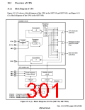
Crystal
oscillator
XTAL
EXTAL
MD8
Peripheral module
clock (Pø) cycle
Pcyc
Bus clock (Bø)
cycle Bcyc
PLL circuit 2
× 1
CKIO
CPG control unit
MD2
MD1
MD0
Standby control
circuit
Clock frequency
control circuit
FRQCR
STBCR
STBCR2
Bus interface
Internal bus
FRQCR: Frequency control register
STBCR: Standby control register
STBCR2: Standby control register 2
Figure 10.1 (2) Block Diagram of CPG (SH7750R)
Rev. 6.0, 07/02, page 250 of 986

 RENESAS [ RENESAS TECHNOLOGY CORP ]