APPENDIX
Appendix 2. Control registers
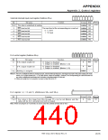
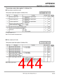
Three-phase output data register 0 (Address A816
)
ꢀ Three-phase waveform mode
b7 b6 b5 b4 b3 b2 b1 b0
Three-phase output data register 0 (Address A816
)
X
X
Bit
0
Bit name
Function
At reset R/W
Reference
10-9
W-phase output fix bit
0 : Released from output fixation
1 : Output fixed
0
RW
V-phase output fix bit
U-phase output fix bit
0 : Released from output fixation
1 : Output fixed
1
2
3
0
0
0
RW
RW
RW
0 : Released from output fixation
1 : Output fixed
W-phase output polarity set buffer
(Valid in three-phase mode 0.)
(Note)
0 : “H” output
1 : “L” output
0
0
RW
RW
Invalid in the three-phase waveform mode.
5, 4
6
b7 b6
Clock-source-of-dead-time-timer
0 0 : f
0 1 : f
1 0 : f
2
2
2
/2
/4
select bits
7
0
RW
1 1 : Do not select.
X: It may be either “0” or “1.”
Note: This bit is invalid in three-phase mode 1.
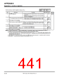
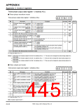
ꢀ Pulse output port mode
b7 b6 b5 b4 b3 b2 b1 b0
Three-phase output data register 0 (Address A816
)
Bit
0
Bit name
Function
At reset R/W
Reference
RTP0
RTP0
RTP0
0
1
2
pulse output data bit
9-7
0
0
0
0
0
RW
RW
RW
RW
RW
0 : “L” level output
1 : “H” level output
pulse output data bit
pulse output data bit
1
2
3
RTP0
3
0
pulse output data bit
pulse output data bit
(Valid in pulse mode 1.) (Note) 1 : “H” level output
RTP1
0 : “L” level output
4
5
RTP1 pulse output data bit
(Valid in pulse mode 1.) (Note)
1
0
0
RW
RW
b7 b6
Pulse output trigger select bits
7, 6
0 0 : Underflow of timer A0
0 1 : Falling edge of input signal to pin RTPTRG0
1 0 : Rising edge of input signal to pin RTPTRG0
1 1 : Both falling and rising edges of input signal to
pin RTPTRG0
Note: Invalid in pulse mode 0.
7906 Group User’s Manual Rev.2.0
20-39

 RENESAS [ RENESAS TECHNOLOGY CORP ]