APPENDIX
Appendix 2. Control registers
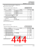
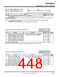
Timer A0
Timer A1
Timer A2
1
1
1
register (Addresses D116, D016
register (Addresses D316, D216
register (Addresses D516, D416
)
)
)
(b8)
b0 b7
(b15)
b7
b0
Reference
Bit
Function
Any value in the range from 000016 to FFFF16 can be set.
At reset R/W
10-13
15 to 0
Undefined WO
Assuming that the set value = n, the “H” level width of the one-shot pulse is expressed
as follows: n/f
: Frequency of a count source
i.
f
i
Notes 1: Use the MOVM or STA (STAD) instruction for writing to this register. Additionally, make sure writing to this register
must be performed in a unit of 16 bits.
2: This register is valid only in three-phase mode 1 of the three-phase waveform mode.
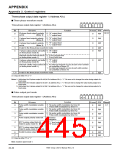
b7 b6 b5 b4 b3 b2 b1 b0
Comparator function select register 0 (Address DC16
)
0 0
0
Reference
Bit
0
Bit name
Function
At reset R/W
12-9
0 : The comparator function is not selected.
1 : The comparator function is selected.
AN
AN
AN
AN
AN
0
1
2
3
4
pin comparator function select bit
pin comparator function select bit
pin comparator function select bit
pin comparator function select bit
pin comparator function select bit
0
0
0
0
0
0
RW
RW
RW
RW
RW
RW
1
2
3
4
7 to 5 Fix these bits to “000.”
Note: Writing to comparator function select register 0 must be performed while the A-D converter halts.
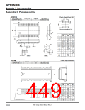
b7 b6 b5 b4 b3 b2 b1 b0
Comparator result register 0 (Address DE16
)
0 0 0
Bit
0
Bit name
Function
At reset R/W
Reference
12-9
0 : The set value > The input level at pin AN
1 : The set value < The input level at pin AN
i
i
AN
AN
AN
AN
AN
0
1
2
3
4
pin comparator result bit
pin comparator result bit
pin comparator result bit
pin comparator result bit
pin comparator result bit
0
0
0
0
0
0
RW
RW
RW
RW
RW
RW
1
2
3
4
7 to 5 Fix these bits to “000.”
Note: Writing to comparator result register 0 must be performed while the A-D converter halts.
7906 Group User’s Manual Rev.2.0
20-43

 RENESAS [ RENESAS TECHNOLOGY CORP ]