APPENDIX
Appendix 2. Control registers
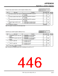
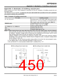
b7 b6 b5 b4 b3 b2 b1 b0
Position-data-retain function control register (Address AA16
)
Bit
0
Bit name
Function
At reset R/W
Reference
Input level at pin IDW is read out.
0 : “L” level
10-12
W-phase position data retain bit
0
0
0
RO
RO
RO
1 : “H” level
Input level at pin IDV is read out.
0 : “L” level
V-phase position data retain bit
U-phase position data retain bit
1
2
1 : “H” level
Input level at pin IDU is read out.
0 : “L” level
1 : “H” level
0 : Falling edge of positive phase
1 : Rising edge of positive phase
3
Retain-trigger polarity select
bit
0
RW
—
7 to 4 Nothing is assigned.
Undefined
Note: This register is valid only in the three-phase mode.
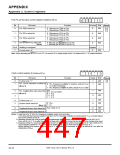
b7 b6 b5 b4 b3 b2 b1 b0
At reset R/W
Serial I/O pin control register (Address AC16)
Reference
Function
Bit
0
Bit name
11-17
0 : CTS0/RTS0 are used together.
1 : CTS0/RTS0 are separated.
0
RW
RW
RW
CTS0/RTS0 separate select bit
(Note)
0 : CTS1/RTS1 are used together.
1 : CTS1/RTS1 are separated.
CTS1/RTS1 separate select bit
1
2
0
0
0
0
(Note)
TxD0/P13 switch bit
0 : Functions as TxD0.
1 : Functions as P13.
RW
—
0 : Functions as TxD1.
1 : Functions as P17.
3
TxD1/P17 switch bit
7 to 4
The value is “0000” at reading.
Note: Valid when the CTS/RTS enable bit (bit 4 at addresses 3416 and 3C16) is “0.”
7906 Group User’s Manual Rev.2.0
20-41

 RENESAS [ RENESAS TECHNOLOGY CORP ]